Détecteurs Cryogéniques et instrumentation associée - Séminaire thématique GT08 "Détecteurs et instrumentation associée " Prospective IN2P3 2020 ...
←
→
Transcription du contenu de la page
Si votre navigateur ne rend pas la page correctement, lisez s'il vous plaît le contenu de la page ci-dessous
Détecteurs Cryogéniques et
 instrumentation associée

 Séminaire thématique GT08
 "Détecteurs et instrumentation associée »
 Prospective IN2P3 2020

 Alex Juillard IP2I
contribution APC, IP2I, LPSC, CSNSM et Institut Néel
Plan
✦ Détecteur cryo ?
✦ Exemple de réalisation
 • EDELWEISS
 • CUPID-Mo
 • NIKA2
 • QUBIC
✦ Prospectives R&D
 • bolo massif & matrice
✦ Conclusion

 2
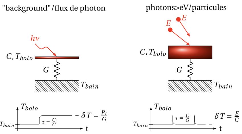
Détecteur cryo ??
 Thermomètre

 ?
 Absorbeur Thermomètre
 « transforme » T en
 Bolomètre « massif » grandeur mesurable
 Matrice de Bolomètre
✦ ~ g ➙ ~ kg ✦ Résistif
 ✦ 1 ➙ 100k « pixels » • supraconducteur
✦ procédé de fabrication en ✦ procédé de fabrication en • Transition Métal-Isolant
 partie « à la main » partie « collectif » ✦ Magnétique
✦ détection de particule ✦ détection de particule ✦ avec médiateur hors
 « une à une » « une à une » ou flux de d’équilibre
✦ application principale : puissance • Paire de Cooper dans
 détection ✦ application principale : matériaux supra :
 d’ »événements rares » • Kinetic Inductance vs dNqp
 Astro • phonon hors d’équilibre
 • Matière Noire • Sub-mm (50-600 Ghz) peuvent « casser « des paires
 • 0 ββ • X de Cooper

 • CE NS 3
D. Prêle DRTBT 2018
 Détecteur cryo ??

 Mode « bolométrique » Mode « calorimétrique »
 ✦ Réponse en C/G ✦ Décroissance en C/G
 ✦ NEP = √4kBT2G [W/√Hz] ✦ δE = √4kBT2C [J]

 Il faut refroidir : sensibilité ➚ et bruit ➘
 Tbain ~10 mK - 300 mK

 R&D = absorbeur + thermomètre + electronique (adaptation Z, gain, readout) +
 environnement cryo 4
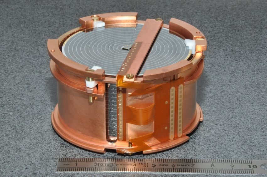
Ex. de réalisation : EDELWEISS-III

 2017 JINST 12 P08010
 SM
 SN
 IC
 2
 IP
 36 * FID-800
✦ Ge 820 g
✦ Thermomètres haute
 impédance Ge-NTD
 (cristal Ge dopé par
 neutron)
✦ 4 jeux d’électrodes Al pour INSTRUMENT (> 2013)
 collecte charge ✦ Cryostat 10mK + 40 tonnes blindages PE + Pb @ LSM
 • Mesure simultanée ✦ 3000 cables coaxes (6 km)
 ionisation - chaleur ✦ 350 transistors Si-FET @ 120K
 • Discrimination active ✦ 36*2 « Bolometers Boxes » @ 300K
 du fond 5
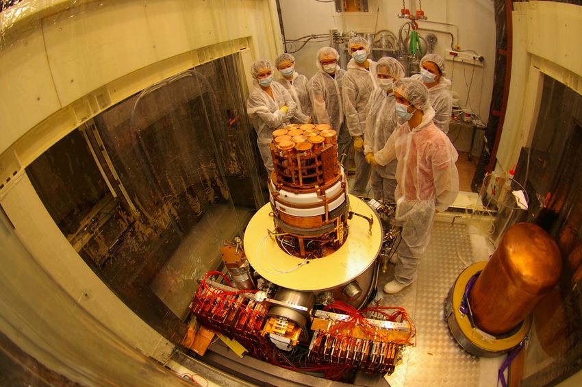
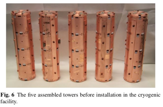
Ex. de réalisation : CUPID-Mo

 https://arxiv.org/abs/1909.02994

 L
 LA
 5 tours de 4 detecteurs (2018)

 SM
✦ Absorber Li2100MoO4: Ø 43.8 x 45

 SN
 mm, 210 g
 Light detector: Ge wafer Ø 44.5 mm x
 IC
✦
 170 μm with SiO coating
 2
 IP

✦ Thermomètre Ge-NTD
✦ Mesure simultanée chaleur - lumière
 pour discrimination fond alpha
✦ Cu basse radioactivité

 Cryostat, Electronique & DAQ
 EDELWEIS-III 6
 6
Ex. de réalisation : NIKA2
A&A 609, A115 (2018)

 SC
 LP
 l
 ée
 N
 I.

 3 Matrices de KIDS (kinetic inductance det.)
 ✦ Cryostat 150 mK
 ✦ 3000 pixels. 150 & 260 GHz
 ✦ Only 20 feed lines and 20 HEMT LNA@4K !
 ✦7 LPSC 300K elec. 7
Ex. de réalisation : QUBIC

 https://arxiv.org/abs/1812.00785
 L
 LA
 SM
 SN
 C
 PC
 A Démonstrateur
 Technologique@APC
 déploiement possible en Argentine
 (2020)
 ✦ Interférométrie bolométrique
 ✦ Cryostat 300 mK
 ✦ 248 pixels NbSi supra (2000 sur
 Inst. final).
Matrice NbSi TES ✦ 150 GHz ( + 220 GHz sur Instr. final)
 (CSNSM) ✦ Custom squids + ASIC cold
 elec (AMS 0.35 SiGe)
 8
 ✦ 128:1 multiplexage
 8
Prospective R&D : senseurs thermiques Ge-NTD

 EDELWEISS FID800 det.
 Ge-NTD (CSNSM, IP2I)
Semiconducteur dopé par neutron. Proche de la transition métal
 isolant.
✦ Production de NTD auprès de réacteur de
 recherche possible en France
✦ Production récente (2015) dans le cadre de
 l’ANR LUMINEU (CSNSM - CEA)
✦ Pas de nouvelle production envisagée. Contact

 https://arxiv.org/abs/1909.02994
 avec d’autres filières.
✦ R&D : Optimisation
 • découpe, métallisation. collage.
 • Gros travail de sélection et de mesure de
 possible bruit en excès
 • préparer les besoins futurs (1000s of
 NTDs sur 10 ans)
 R (MΩ)

 9
Prospective R&D : senseurs thermiques NbSi

 17000 NbSi-Al cells in series to form a spiral

 Stefanos Marnieros & CSNSM
 120µm

 24µm

 Basse Impédance Haute Impédance
 Al on NbSi NbSi

 NbxSi1-x (CSNSM)
 Other tested
Alliage proche de la transition métal-isolant ou supra designs … 80µm
 40µm
 5µm
 10µm
 100µm 50µm 50µm
 2µm
 10 µm, 5 µm 10µm
✦ > 20 ans de développement. Co-évap film and 2 µm TES 2µm 5µm

 10µm

 mince
 10

✦ Convergence vers supra haute ou basse
 impédance
✦ Techniques de micro-lithography (CNRS/
 C2N) adaptées pour matrices de
 détecteurs (QUBIC) ET bolomètres
 massifs (EDELWEISS, Ricochet).
✦ R&D : Four Si wafers with several phonon-trap
 • minimiser la chaleur spécifique en alternant les designs were realized

 parties senseurs et pièges à phonons Samples with TES islands ≥ 5 µm are OK
 Samples with 2 µm TES have some problems
 • veto pour événements de surface de basse énergie
 (états supra« metastable »)
 10
Prospective R&D : senseurs KIDs
 We can detect
 incident power
 Kinetic Inductance Detector by monitoring

 Alicia Gomez DRTBT2018
 the resonance
 (I. Néel, LPSC, APC) LC
 superconducting
 Capacitor
 resonator
 = Résonateur supraconducteur >

✦ Résonance dépend de la densité de paire de ns nqp
 Cooper : sensible à tout dépôt E>∆s
✦ Initié en 2000 par Caltec/JPL LK R

✦ gros driver France : NIKA2 + Néel group =

 Inductor
✦ R&D : ′ =

 ′
 • haut niveau d’integration : JPL-Caltech (2001) – P. Day, J. Zmuidzinas

 R&D KIDs = R&D détecteur
 • Pour le moment techno Al mature mais
 Multiplexing 1 wire >1000 KIDs
 bande passante limitée (gap supra)
 • Objectif : élargir la bande à 50 - 650 GHz
 ➡ diminuer Tc (Tc Al = 1.4K) Transmission line

 ➡ Al-Ti ou autre matériaux
 = =

 • Sensibilité au phonons
 ➡ detection de particule (IP2I)

 = =

 500 mm 11
Prospective R&D : Bolomètre massif

3 développements principaux :
✦ 0ν2β (désintégration double beta sans emission de neutrino) :
 préparer la suite de CUORE = CUPID
 ➡ CUPID-Mo @ LSM
 ➡ objectif 1 tonne de detector avec discrimination active du fond

✦ « Crise » de la Matière Noire : aucun signe de détection directe + absence de
 nouvelle physique au LHC
 ➡ « Fin » du WIMPs standard, Elargir la recherche (EDELWEISS-SubGeV)

✦ Recherche de nouvelle physique via mesure fine CE NS (Coherent Elastic
 neutrino-nucleus scattering)
 ➡ pousser la discrimination à très bas seuil (Ricochet)

✦ Nombreuses autres applications :
 ➡ Spectro neutrons rapides, observation décroissance rare, métrologie, etc.

 12
Prospective R&D : CUPID

 https://arxiv.org/abs/1712.07995
 CUPID
 CUORE Upgrade with Particle Identification

✦ 30 instituts, 100aines de personnes
✦ Long processus de selection des R&D
 • https://arxiv.org/abs/1504.03612
✦ R&D France (CUPID-Mo, CSNSM-IP2I-
 LAL + CEA) sélectionnée comme
 base de CUPID
 • https://arxiv.org/abs/1907.09376
✦ Projet CROSS CUORE @ LNGS
✦ Détails dans contribution au GT06
✦ programme à ~10 ans

 https://arxiv.org/abs/1504.03612
 13
Prospective R&D : EDW-Sub GeV
 « small is beautiful ! »
✦ Pas d’observation de WIMPs « standard » (M> qq
 GeV) avec des taux d’interactions < 1 evt/tonne/
 an !
✦ Les détecteurs cryo ne sont plus compétitifs dans
 cette zone
✦ Intrinsèquement compétitif à basse masse (résolution
 et seuil)
✦ bonne nouvelle : si DM = Sub-GeV WIMPs il y en a
 donc beaucoup plus !
 • 1 kg de « bons » détecteurs est compétitif
 R&D « HEMT » Mesures@LSM
✦ Axion & ALPs : Reculs électroniques commune avec (proto)
 • ! fond parasite « chaleur seule » Ricochet
✦ Objectif R&D : IPNL CSNSM (+ CEA) Effet Luke « boosté », sens. paire unique
 • Tenue en tension (courant fuite) pour
 « boost » effet Luke
 • Discrimination jusqu’à la paire e-/h+
 unique
 • Changement de technologie elec.
 froid
 ➡ Si-JFET ➛ HEMT (C2N/CNRS)

✦ programme à ~ 5 ans
 14
Prospective R&D : Ricochet Journal of Low Temperature Physics

 91 eVee baseline RMS ionization resolution with a HEMT-based cryogenic charge
 amplifier with a 240g CDMS-II cryogenic germanium detector, nearly matching the
 model predictions. However, the complexity required to implement a HEMT-based
Mesure de précision d’un signal connu ! fully cryogenic charge amplifier for the hundreds of ionization channels present in a
 reasonably sized experiment requires us to explore amplifier topologies where the use
 IPNL, CSNSM, LPSC, I. Néel of cryogenic HEMTs is limited to only the input transistor.
 Two schemes are thus being investigating : (1) a simple follower HEMT-based stage
 at 1–4 K, very close to the detector with a very low noise 300 K stage and (2) an hybrid
✦ changement de philosophie après la HEMT + SiGe / MOS ASICs high gain stage at 1–4K. The follower scheme is used
 by the EDELWEISS collaboration [1,26] and works are in progress to adapt it to an
 Matière Noire HEMT input. A production of ASICs based on the 0.35 µm SiGe biCMOS technology
 from AMS foundry has been delivered and will be tested soon. This technology has
✦ Mesure du CE NS pour de 5 MeV demonstrated T = 4.2 K performances [28]. SiGe bipolar transistors will be used
 for amplification, and pMOS/nMOS switches will be used for calibration and reset
 (mesuré en 2018 @ 30 MeV) purposes.

✦ Cahier des charges « simple » 5 Conclusion: Prospect for a 10 eV Heat, 20 eVee Ionization, 35 g
 Germanium Cryogenic Detector
 • 1 kg Ge (27*38g)
 The EDELWEISS collaboration has recently demonstrated an impressive 18 eV RMS
 • 20 eV ioni + 10eV chal
 Réacteur
 heat resolution on a 3460 MWdetector
 g germanium @ [11].
 ILL / Grenoble
 Careful analysis has shown that the
 resolution is limited by the current noise of the Si-JFET. Our HEMT model predicts
✦ R&D en partie techno (transistor HEMT) ✦ than
 Installation
 10 eV heat resolutionRicochet
 would be achievableprévue 2022-23
 by simply replacing the JFET with a
 230 pF CNRS/C2N HEMT.
 et commune avec EDELWEISS Journal of Low Temperature Physics
 ✦ programme à ~ 5 ans

 ArXiv 1909.02879
 Ge-NTD Thermal Sensor Heat
 Veto Top
 Interdigitized Al Electrodes
 Fiducial Top

 Field (V)
 10 mm
 15 mm
Fig. 5 Left: Contribution to the ionization resolution of the voltage noise, current noise, bias resistor (10
G! @ 20 mK). The total detector + cabling capacitance is 20 pF. 5 pF and 100 pF geometries have Fig. 6 Electrostatic simulation of a Full Inter-Digitized electrodes scheme on a 38 g germanium crystal
been studied. FFT of 1 keV event are shown. Right: Evolution of the resolution with the detector + cabling (Φ = 30 g, h = 10 mm). The crystal is surrounded at 2 mm distance by a chassis connected to the ground (not
capacitance for the 5 HEMT geometries and the IF1320 Si-JFET from InterFET. Noise of the bias resistor shown). The capacitance of the 4 electrodes with respect to the ground is about 20 pF (Color figure online.)
is included. (Color figure online.) 15
Prospective R&D : Instruments astro sub-mm

 Prospective IN2P3 GT05 :
✦ Short-term goal (2019-2020):
 • Maintain KID activity with existing instrument NIKA2
 and KISS ensuring upgrades to increase the
 performance.
 • Install QUBIC at 5000m site in Salta province,
 Argentina. Demonstrate Bolometric Interferometry on
 sky data

✦ Mid-term goal (2020-2024):
 • installation of CONCERTO (KIDs, 2021). Maintain the
 observations for several years.
 Begin studying the design for S4-like instruments.
 • Data taking with QUBIC Technical Demonstrator.
 Upgrades: Multimode horns, 400 horn array, additional
 focal plane for 220GHz

✦ Long-term goal (2024-2030):
 • be ready to answer to the expectations of the S4
 network. Be a valid candidate for covering the focal
 plane of the next generation space mission devoted
 to the CMB
 • Large QUBIC-like instrument with KID detector array,
 proposed as part of the S4 collaboration
 • Bolometric Interferometer in the focal plane of LLAMA
 16
Prospective R&D : QUBIC
Universe 2019, 5, 42

 arxiv:1609.04372

 Démonstrateur Technologique @ APC
JLTP 2019

 = 1/8 Instrument Final @ La Puna
 (Argentina)
 ✦ programme à ~ ? ans
 ✦ décision de déploiement sur site en
 attente
 17
Prospective R&D : KISS & Concerto
 u is
 e p
 é d
 t a ll
 018
 2
 Ins fin

 « Pathfinder pour CONCERTO et spectre MPI »

 Installation 2021

 18
R&D Readout : discret & ASICs
✦ Les
 détecteurs cryogéniques nécessitent une électronique de lecture
 spécifique (cryo + 300K)
✦ Développements discrets (HEMT, JFET, SQUID) et ASIC (cf session
 dédiée demain) :
 • Multiplexeur CMOS AMS 0.35 T bande GHz
 • ➚ nombre de pixel, convergence readout KIDs-TES

 19
Conclusion
✦ Les détecteurs cryogéniques sont arrivés à maturité et sont intégrés
 dans des instruments complexes.
✦ Qq grands projets fédérateurs bien identifiés sur les 10 prochaines années

Remarques « ITA » :
✦ Effet ANR / Labex / ERC : foisonnement de projets avec des objectifs à
 court-terme.
 • Au final peu de contrôle a priori sur cette explosion par l’IN2P3
 (incitation à la recherche de financement de ce type)
 • Saturation des services techniques
✦ L’IN2P3 met-elle vraiment les moyens suffisants pour ses ambitions
 « spatiales » ?
✦ Développements longs : Maintien des compétences sur la durée
 difficile
 • Nombreuses taches techniques assurées par des post-docs et CDD
✦ Pas certain qu’une couche supplémentaire de sélection darwinienne mette
 de l’huile dans la machine…

 20
Standard technological Process :
Clean Room
 On a 4 inch silicon mono crystalline and high
 purity (> 1000Ω.cm) wafer, a thin layer (18nm)
 of aluminium is coated by electron beam
 evaporator (under a residual vacuum 5.108 mbar)

 Print patterns via optical lithography (λ = 365nm)
 through a dedicated mask

 The metal is etched by a chemical (phosphoric
 acid) solution through resist apertures.

Hard points: The homogeneity of the aluminum layer, have a
full 4 inch surface without major defects (dust, bubbles)

 21
Standard technological Process:
Packaging

 Dicing the edges of the array, and structure the
 backside of array to add a function of optical
 adaptation layer (AR).

 The AR strategy is to reduce the silicon density
 by grooves to obtain an effective index
 nvoid = 1 < nadapt ~ 2 < nSi ~ 3.4

 After mounting in a dedicated holder, connect the
 feedlines and improve the equipotentiality of the
 ground plan by sticking small bridges above the
 signal line (25µm diameter wires).

 22
NbSi array for QUBIC

 Pixel architecture.
 Fabrication by micro-lithography.
 (IJCLab-C2N)

 NbSi - TES

250 pixel array for QUBIC. High sensitivity TES with adjustable TC .
(full focal plane = 4 arrays)

 Bonding & integration of the array

 Deep silicon etching on the backside
 to realise the suspended membrane
 of the pixels.
 High thermal decoupling to optimise
 signal/noise of the detector.

 23
Vous pouvez aussi lire