PROGRAMME - Journées Plénières du GDR NEMO
←
→
Transcription du contenu de la page
Si votre navigateur ne rend pas la page correctement, lisez s'il vous plaît le contenu de la page ci-dessous

PROGRAMME

    1
Membres du Conseil Scientifique
Amandine BELLEC
Laboratoire Matériaux et Phénomènes Quantiques (MPQ) UMR 7162 – Paris
Marie Laure BOQUET
Laboratoire de physique de l’ENS (LPENS) – UMR 8023, Paris
Xavier BOUJU
CEMES – UPR 8011, Toulouse
Stéphane CAMPIDELLI
Laboratoire d’Innovation en Chimie des Surfaces et Nanosciences (LICSEN)
DRF/IRAMIS/NIMBE (UMR 3685) – Saclay
Frédéric CHERIOUX
Institut Franche-Comté électronique mécanique thermique et optique – sciences et technologies (FEMTO-ST)
– UMR 6174, Besancon
Saioa COBO
Département de Chimie Moléculaire (DCM) – UMR 52550, Grenoble
Johann CORAUX
Institut Néel – UPR 2940, Grenoble
Jean-François DAYEN
Institut de Physique et Chimie des Matériaux de Strasbourg (IPCMS) – UMR 7504, Strasbourg
Bruno FABRE
Institut des Sciences Chimiques de Rennes – UMR 6226, Rennes
Benoit HACKENS
Université Catholique de Louvain, Louvain (Belgique)
Jean Christophe LACROIX
Interfaces, Traitements, Organisation et Dynamique des Systèmes (ITODYS) – UMR 7086, Paris
Philippe LECLERE
Laboratory for Chemistry of Novel Materials, Mons (Belgique)
Richard MATTANA
Unité Mixte de Physique CNRS/Thales (UMPhy) – UMR137, Saclay
Anna PROUST
Institut Parisien de Chimie Moléculaire UMR 8232 – Sorbonne Université – Paris
Patrice RANNOU
Laboratoire d’Electrochimie et de Physicochimie des Matériaux et des Interfaces (LEPMI) – UMR 5279,
Grenoble
Paolo SAMORI
Institut de science et d’ingénierie supramoléculaires (ISIS) – UMR 7006, Strasbourg
Pierre SENEOR
Unité Mixte de Physique CNRS/Thales (UMPhy) – UMR137, Saclay
Olivier SIRI
Centre Interdisciplinaire de Nanoscience de Marseille (CINaM) – UMR7325, Marseille
Dominique VUILLAUME
Institut d’électronique, de microélectronique et de nanotechnologie (IEMN) – UMR 8520, Lille
Jean WEISS
Institut de Chimie de Strasbourg – UMR 7177, Strasbourg

                                                    2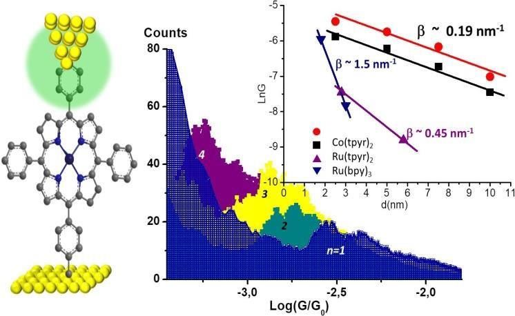
Conférenciers Invités

Axe 1 - Systèmes molécule unique,                          Axe 2 - Jonctions à plus large échelle,
mémoires et switches                                       mémoires et switches

Dr. Christian Joachim                                      Prof. Jean-Christophe Lacroix
CNRS - Université de Toulouse                              Université Paris Cité

Axe 3 - Matériaux & Ingénierie                             Axe 4 Transverse - Outils de
moléculaire                                                caractérisation et de modélisation

Dr. Saioa Cobo                                             Prof. Marie-Laure Bocquet
Université Grenoble Alpes                                  Ecole Normale Supérieur

Membres du Bureau

     Pascal Martin               Yannick Dappe                 Stéphane Lenfant         Maria Luisa Della Rocca
    Directeur du GDR        Directeur adjoint du GDR       Directeur adjoint du GDR      Laboratoire MPQU
   Laboratoire ITODYS        Laboratoire SPEC, CEA,            Laboratoire IEMN                MR 7162
       UMR 7086                       CNRS                        UMR 8520               Université Paris Cité
   Université Paris Cité     Université Paris-Saclay           Université de Lille

      Laurent Limot                Denis Frath                    Neus Vila                  Vincent Huc
   Laboratoire IPCMS             Laboratoire LCH             Laboratoire LCPME            Laboratoire ICMMO
        UMR 7504                    UMR 5182                     UMR 7564                     UMR 8182
 Université de Strasbourg          ENS de Lyon              Université de Lorraine       Université Paris Saclay

                                                       3
Programme
                                   Lundi 26 septembre 2022
08h30           Accueil
09h00           Présentation du GDR NEMO
09h10           Invité - Christian Joachim
        A1

                From the single molecular rectifier to a full digital adder in a single molecule
09h50           Pause café
10h20           Rémi Avriller
                Photon-emission statistics induced by electron tunneling in plasmonic nanojunctions
10h40           Amandine Bellec
                Voltage-Induced Bistability of Single Spin-Crossover Molecules in a Two-Dimensional
                Monolayer
11h00           Cyrille Barreteau
        Axe 1

                Spin manipulation and detection at the single molecule scale: Towards a new concept of
                device in molecular spintronics
11h20           Xiaonan Sun
                Single Molecule Junctions from Metal-Complex Molecules: Long range charge transport,
                stability and I/V characteristics
11h40           Lionel Patrone
                Self-assembled monolayers on Ge as passivating & insulating films
12h00           Déjeuner
13h30           Invité - Jean-Christophe Lacroix
                Electrochemistry does the impossible: Robust and Reliable Molecular Junctions
14h10           Anna Proust
        Axe 2

                Manipulating Polyoxometalates at the nanoscale: charge transport in POM-based
                molecular junctions
14h30           Stéphane Rigaut
                Molecular Electronics with Organometallic Complexes as Wires and Switches
14h50           Pause café
15h20           Clément Barraud
                Spin filtering effects through graphene/molecules heterostructures
15h40           Dominique Vuillaume
                Molecule-Nanoparticle 2D networks for neuro-inspired computing: concepts, results and
                perspectives
16h00           Bruno Fabre
        Axe 2

                Functionalized Silicon Surfaces for the Development of Light-Activated Molecular
                Electronics Devices
16h20           Mathieu Gonidec
                Switchable spin-crossover molecular junctions
16h40           Benoît Gobaut
                Quantum information encoding & Energy harvesting using molecular spintronics
17h00           Table ronde
18h30           Cocktail

                                                  4
Programme
                                  Mardi 27 septembre 2022
08h30           Invité - Saioa Cobo
                Matériaux & Ingénierie moléculaire : de la molécule unique au dispositif
09h10           David Kreher
        Axe 3

                New TADF emitters based on pyridazine for OLEDs applications
09h30           Jérôme Lagoute
                Nanostructuration of nitrogen dopants in graphene with a submonolayer molecular
                resist to form sharp junctions
09h50           Pause café
10h20           Christophe Bucher
                Manipulating Molecules with Electrons: From Machines to Responsive Soft Materials
10h40           Amparo Ruiz-Carretero
                Exploring the role of hydrogen-bonding and supramolecular chirality in organic
                electronics
        Axe 3

11h00           Frédéric Lafolet
                From electrografted layers to molecular junctions based on coordination complexes
11h20           Nataliya Kalashnyk
                Reactivity and selectivity of homo-coupling reactions driven by surface orientation and
                temperature
11h40           Rodrigue Lescouëzec
                Équipe de Recherche en Matériaux Moléculaires et Spectroscopie
12h00           Déjeuner
13h30           Invité - Marie-Laure Bocquet
                Interfaces fonctionnelles en UHV et dans l’eau : apports récents des simulations ab initio
        Axe 4

14h10           Jérôme Cornil
                Theoretical Insight into the Electronic Properties of Functional Molecular Junctions
14h30           Karine Costuas
                Computational design of molecular systems for nano-thermoelectric applications
14h50           Pause café
15h10           Dongzhe Li
                Negative differential resistance in spin crossover molecular devices
15h30           Christophe Krzeminski
        Axe 4

                Modélisation Physique d’Interrupteur Moléculaire
15h50           Alexander Smogunov
                Simulations ab initio des phénomènes de transport et dynamique quantique dans des
                nanostructures
16h10           Table ronde - Conclusion
16h40           Clôture des premières journées plénières du GDR Nemo

                                                 5
From the single molecular rectifier
                        to a full digital adder in a single molecule
                                               Christian Joachim
                    Centre d’Élaboration de Matériaux et d’Études Structurales (CEMES-CNRS),
                Université de Toulouse, 29 Rue J. Marvig, BP 94347, 31055 Toulouse Cedex, France.
                                                joachim@cemes.fr

Abstract:
We have 50 years. From the first IBM patent in molecular electronics [1] and the 1974 A. Aviram and M.
Ratner publication proposing a single molecule molecular rectifier [2] to its recent merging with quantum
engineering and the quantum Hamiltonian computing (QHC) approach [3,4] (already anticipated in the
80’s [5]), a lot of avenues have been explored for single molecule molecular electronics [6]: chemistry [7]
and surface science [8], nanolithography reaching 5 nm co-planar metal nano-junctions [9],
instrumentations with the new LT-UHV 4-STM [10], nano-packaging with UHV compatible back
interconnects [11] and quantum chemistry with the multi-channels molecular orbital basis set Elastic
Scattering Quantum Chemistry (ESQC) calculations of a tunneling current intensity and its CI-ESQC
generalization [12]. The objective is now for a single molecule to be not only a switch [13] or an amplifier
[14] or a classical electronic circuit [15] but finally a quantum digital calculator by itself [16]. From time to
time and along those 50 years, new fields emerged like single molecule mechanical machines [17] and
more fundamental questions arise like the STM-STS mapping (or not) of molecular orbitals [18] or the
chase of the elusive super-tunneling effect [19,20].
References:
 [1]: A. Aviram, P.E. Seiden, Patent filed 20th June 1973, No.: 371,788 1973, USPTO No: 3,833,894
 [2]: Aviram, M. Ratner, Chem. Phys. Lett. 29, 277, (1974).
 [3]: W.H. Soe and coll., ACS Nano, 5 ,1436 (2011).
 [4]: P. W. K. Jensen and coll., Quantum Sci. Technol. 4, 015013 (2019).
 [5]: C. Joachim, J.P. Launay, “Molecular Electronics Devices” p. 149, Ed. F.L. Carter (Elsevier, 1988).
 [6]: C. Joachim, J. K. Gimzewski and A. Aviram, Nature 408, 541 (2000).
 [7]: J.P. Launay, Chem. Soc. Rev., 30, 386 (2001).
 [8]: G. Franc, A. Gourdon, Phys Chem Chem Phys, 131,14283 (2011).
 [9]: M. S. M. Saifullah, T. Ondarçuhu, D. F. Koltsov, C. Joachim, M. Welland, Nanotechnology, 13, 659 (2002).
[10]: J. Yang, D. Sordes, M. Kolmer, D. Martrou and C. Joachim, Eur. Phys. J. Appl. Phys. 73, 10702 (2016).
[11]: D. Sordes and coll., Springer Series: “Advances Atom and Single Molecule Machines”: Vol. IX, p. 25 (2017).
[12]: M. Portais, C. Joachim, Chem. Phys. Lett., 592, 272 (2014).
[13]: A. Aviram, C. Joachim, M. Pomerantz, Chem. Phys. Lett., 146, 490 (1988).
[14]: C. Joachim et J.K. Gimzewski, Chem. Phys. Lett., 265, 353 (1997).
[15]: J. C. Ellenbogen, J. C. Love, Proc. IEEE, 88, 386 (2000).
[16]: W.H. Soe, P. de Mendoza, A.M. Echavarren, C. Joachim, J. Phys. Chem. Lett, 12, 8528 (2021).
[17]: J.K. Gimzewski, C. Joachim, R.R. Schlittler, V. Langlais, H. Tang, J. Johanson, Science, 281, 531 (1998).
[18]: J. Repp, G. Meyer, S. Stojkovic, A. Gourdon, C. Joachim, Phys. Rev. Lett., 94, 026803 (2005).
[19]: C. Joachim, M. Ratner, PNAS, 102, 8801 (2005).
[20]: D. Skidin and coll., Nanoscale, 10, 17131 (2018).

                                                         6
Photon-emission statistics induced by electron tunneling in
                       plasmonic nanojunctions

                 R.Avrillera , Q. Schaeverbekea,b , T. Frederiksenb ,c, and F. Pistolesi a
                 a
                     Univ. Bordeaux, CNRS, LOMA, UMR 5798, F-33405 Talence, France. bDonostia
                        International Physics Center (DIPC), E-20018 Donostia-San Sebastián.
                         c
                          Ikerbasque, Basque Foundation for Science, E-48013 Bilbao, Spain.

Abstract:
          We investigate the statistics of photons emitted by tunneling electrons in a single electronic level
plasmonic nanojunction (see Fig.1). We compute the waiting-time distribution of successive emitted
photons         . When the cavity damping rate is larger than the electronic tunneling rate , we show
that in the photon-antibunching regime,              indicates that the average delay time between two
successive photon-emission events is given by        . This is in contrast with the usually considered second-
order correlation function of emitted photons,               , which displays the single timescale       . Our
analysis shows a relevant example for which          gives independent information on the photon-emission
statistics with respect to           , leading to physical insight into the problem. We discuss how this
information can be extracted from experiments even in the presence of a nonperfect photon-detection
yield.

                                                    Figure 1
  Representation of a current-driven STM plasmonic nanojunction. The cavity emits photons upon tunneling of
single electrons across the STM junction. The emitted photons are collected by a detector. Adapted from Ref[1].

References:
[1] R. Avriller, Q. Schaeverbeke, T. Frederiksen, and F. Pistolesi, Phys. Rev. B 104, L241403 (2021).

                                                        7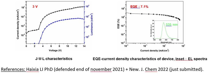
Voltage-Induced Bistability of Single Spin-Crossover Molecules in a
                       Two-Dimensional Monolayer
     Yongfeng TONGa, Massine KELAIa, Kaushik BAIRAGIa, Vincent REPAINa, Jérôme LAGOUTEa,
         Yann GIRARDa, Sylvie ROUSSETa, Marie-Laure BOILLOTb, Talal MALLAHb, Cristian
                               ENACHESCUc, Amandine BELLECa
     a
       Université Paris Cité, CNRS, Laboratoire Matériaux et Phénomènes Quantiques, UMR6271, F-75013, Paris,
                                        France. Email:amandine.bellec@u-paris.fr
     b
       Institut de Chimie Moléculaire et des Matériaux d'Orsay, Université Paris-Saclay, CNRS, UMR 8182, 91405
                                                 Orsay 12 Cedex, France
                    c
                     Faculty of Physics, Alexandru Ioan Cuza University of Iasi, Iasi 700506, Romania

Abstract:
Bistable spin-crossover molecules are particularly interesting for the development of innovative
electronic and spintronic devices as they present two spin states that can be controlled by external
stimuli. Here, we report the voltage-induced switching of the high spin/low spin electronic states of
spin crossover molecules self-assembled in dense 2D networks on Au(111) and Cu(111) by scanning
tunneling microscopy at low temperature.
On Au(111), voltage pulses lead to the non-local switching of the molecules from any - high or low -
spin state to the other followed by a spontaneous relaxation towards their initial state within
minutes.
On the contrary, on Cu(111), single molecules can be addressed at will. They retain their new electronic
configuration after a voltage pulse. The memory effect demonstrated on Cu(111) is due to an interplay
between long range intermolecular interaction and molecule/substrate coupling as confirmed by
mechanoelastic simulations1.

 Figure a) Scheme of the manipulation by voltage-pulses. b) 10x10nm2 and c) 10x12.5nm2 topographic images
                  where “LS” and “HS” have been written by voltage pulses (V=0.3 V, I=3 pA).

References:
1.        Y. Tong et al., J. Phys. Chem Lett., 12, 11029 (2021).

                                                           8
Spin manipulation and detection at the single molecule scale:
         Towards a new concept of device in molecular spintronics
                     Fei Gao,a Dongzhe Li,b Cyrille Barreteau,c Mads Brandbygea
a
  Department of Physics, Technical University of Denmark, DK-2800 Kongens Lyngby, Denmark.
b
  CEMES, Université de Toulouse, CNRS, 29 rue Jeanne Marvig, F-31055 Toulouse, France.
c
 Université Paris-Saclay, CEA, CNRS, SPEC, 91191 Gif-sur-Yvette, France. Email : cyrille.barreteau@cea.fr

Abstract:
Spin manipulation at the nanoscale is a problem of major importance both at the fundamental and
technological levels. Magnetic molecules deposited on a surface offer a unique test bed, but it is
difficult, if not impossible, to explore experimentally the many possible avenues given the huge
combination of molecule/surface systems that exist. This is why modelling plays a key role in this
field. We have shown by computational methods of electronic structure and transport that tetraphenyl
iron porphyrin (FeTPP), deposited on a boron-doped graphene substrate, possesses remarkable
properties that make it a potential candidate for a molecular spintronic device driven solely by the
application of a gate voltage
In particular we showed that FeTPP goes from a spin S=1 to S=3/2 and the iron goes from an
oxidation state Fe2+ to Fe3+ when deposited on B-doped graphene. More interestingly, when a
negative bias voltage is applied the molecule reverts to its S=1 state as on undoped graphene where
the interaction is much weaker and the magnetic polarization disappears on the boron. In addition, this
change can be detected via the spin polarization of the electronic transport through the graphene
sheet.

a) Schematic representation of a FeTPP molecule on a layer of (doped) graphene with an STM tip and a grid
underneath the graphene. b) The two magnetic states (S=3/2 or S=1) of the molecule on boron -doped graphene
that can be reversibly obtained depending on the applied grid voltage. c) Spin polarization of the electronic
transport in the graphene plane: it is 10% without voltage and almost disappears with a negative voltage This
corresponds to 0 or 1 states that can be written with a voltage and read with the current.

We have therefore proposed a new concept for writing and reading spin states at the single molecule
scale using a process that requires an electrical operation (gate voltage) that is much less energy
consuming than the application of a magnetic field or of an intense electric current. This work,
published in Physical Review Letters [1], could pave the way for the development of new low-power
spintronic devices.
References:
[1] “Proposal for all-electrical spin manipulation and detection for a single molecule on boron-substituted
graphene”. Fei Gao, Dongzhe Li, Cyrille Barreteau, Mads Brandbyge. Phys. Rev. Lett. 129, 027201 (2022).

                                                        9
Single Molecule Junctions from Metal-Complex Molecules:
      Long range charge transport, stability and I/V characteristics
Xilei Yao,a Maxime Vonesch, b Frédéric Lafolet,a Jean Weiss, b Xiaonan Sun,a* and Jean-
Christophe Lacroix a*
         a
           ITODYS, CNRS-UMR 7086, Université de Paris Cite, 15 rue Jean-Antoine de Baïf, Paris, France.
                                         Email:sun.xiaonan@u-paris.fr
         b
           Institut de Chimie, CNRS-UMR 7177, Université de Strasbourg, 4 rue Blaise Pascal, Strasbourg
Abstract:
The research of single molecule junction (SMJ) aims to miniaturize the molecular electronics in size and
to optimize the charge transports in efficiency. A SMJ is formed when a single molecule is connected
between two conducting electrodes. We have recently studied SMJs, based on two types of
organometallic oligomers. They are deposited as ultrathin layers on an ultra-flat gold bottom electrode
and are contacted by an STM tip used in various modes (STM-break junction or I(t) mode).
The first systems are based on Au-[metal-(tpy)2]n-Au (n = 1–4). Highly efficient long range transport is
observed from Au-[Co(tpy)2]n-Au SMJs where the conductance (~10-3 G0) shows very weak length
dependence. An extremely low attenuation factor (β∼0.19 nm–1) is obtained which indicates that
resonant charge transport is the main transport mechanism. By varying the SMJ metal center from
Co to Ru, the conductance decreases by 1 order of magnitude. In Au-[Ru(tpy)2]n-Au and Au-
[Ru(bpy)3]n-Au SMJs, a charge transport transition from direct tunneling to hopping is evidenced
from the length-dependent β-plot in the right figure. Three different transports mechanisms are
observed with clear molecular signature. (1)
In a second system, Au-[metal-porphyrine]n-
Au SMJ is studied on both their transport
properties and their stability by recording
the SMJ life time, namely the G(t)
measurements. Au-[NH2-CoTPP]n-Au SMJs
show random telegraph G(t) signals first
then stabilize with a surprisingly long
lifetime around 10s.(2) By adding an extra
NH2 anchoring group, Au-[NH2-CoTPP-NH2]n-
Au SMJs are recorded to stabilize with a life
time as long as 1 min. Thanks to the high stability, intensive I(V) measurements at a single molecule
level are easily feasible. The I/V characteristic from different SMJs indicates that, the applied bias
voltage decreases the attenuation factor and drives the device toward resonant tunneling. (3)
We have therefore obtained SMJs with unprecedented stability and studied their transport
properties using three complementary characterizations: the STM-bj G(d) histogram, the stability
from G(t) and the voltage dependent conductance G(V) measurements. The observed
unprecedented stability is likely due to a combined contribution: the diazonium grafting covalently
immobilizes molecules and impedes molecule movements; the anchoring groups optimize the top
molecule-tip contact.
References:
 [1] X. Yao, X. Sun*, F. Lafolet, J. C. Lacroix*, Nano Lett. 20, 9 (2020) 6899–6907.
[2] X. Yao, M. Vonesch, M. Combes, J. Weiss, X. Sun*, J. C. Lacroix*, Nano Lett. 21, 15 (2021) 6540.
[3] X. Yao, M. Vonesch, J. Weiss, X. Sun*, J. C. Lacroix*, submitted.

                                                        10
Self-assembled monolayers on Ge as passivating & insulating films
Mohamed-Amine Guerboukhaa, Virginie Gadennea, Hela Mrezguiab, Luca Giovanellib, Younal
Ksarib, Guillaume Monierc, Victorien Jeuxd, Jean-Manuel Raimundoe, Lionel Patronea
a
Aix Marseille Univ., Université de Toulon, CNRS, IM2NP UMR 7334, Yncréa Méditerranée, ISEN Toulon, Maison du
Numérique et de l’Innovation, Place G. Pompidou, 83000 Toulon, France - lionel.patrone@im2np.fr
b
Aix Marseille Univ., Université de Toulon, CNRS, IM2NP UMR 7334, 13397, Marseille Cedex 20, France
c
Univ Clermont Auvergne, CNRS, SIGMA Clermont, Inst Pascal, F-63000 Clermont Ferrand, France
d
ESCOM Chimie, 1 allée du réseau JM Buckmaster, 60200 Compiègne, France
e
CINaM UMR CNRS 7325, Aix-Marseille Université, 13288 Marseille cedex 09, France
Ge is emerging as a likely material in the next generation of high-frequency field effect transistors. However, the
preparation of an interfacial layer enabling to passivate and insulate Ge surface is still problematic. A promising
approach consists in designing new self-assembled molecular monolayers (SAMs) [1] grafted on Ge exhibiting highly
insulating and passivating properties as new high-K self-assembled nanodielectrics [2]. We have studied SAMs of
model molecules such as alkylthiols and fluoro-alkylthiols, and of specially synthesized non-charged novel push-pull
chromophores bearing electron donor and acceptor groups, separated by a pi-conjugated bithiophene bridge which
promotes electron transfer and a subsequent dipole formation [3] (Fig. 1a). Indeed, due to the alignment of the
oriented dipoles promoted by the SAM deposition strategy, such push-pull chromophores have been shown to form
highly polarizable insulating films in the literature [2]. We have adapted and developed the original Ge
deoxidation/grafting technique in hydro-alcoholic solution [4] and shown that, compared to the usual deoxidizing acid
treatment, it gives smoother surfaces and well-organized SAMs, which is proven by ellipsometry, wettability, and
scanning probe microscopy analyses. The grafting of alkylthiols and fluoro-alkylthiols on Ge has been performed
directly in a single step, whereas for the push-pull chromophores designed with a carboxylic anchoring group, we have
achieved a two-step grafting with amide bonding on pre-assembled amine-terminated sticking layers. Among the
latter, we have demonstrated aminothiophenol SAMs exhibit a better arrangement than cysteamine, with a smooth
monolayer film suitable for grafting ordered push-pull SAMs on top. UV-Visible absorption spectroscopy of push-pull
chromophores in solution was used to determine the concentration limit to avoid aggregation. X-ray photoelectron
spectroscopy (XPS) and infrared spectroscopy (FTIR) analyses demonstrate the oxide removal from the Ge surface
after the SAM formation (Fig. 1b-c). Statistical electrical analyses revealed that with such push-pull SAMs, we have
been able to decrease the current by a factor of 105 compared to Ge, and 104 compared to dodecane SAMs of similar
thickness (Fig. 1d). Results have been analyzed by transition voltage spectroscopy [5], and successfully correlated with
spectroscopic analyses of molecular levels, using inverse photoemission spectroscopy and XPS valence band
determination for probing the unoccupied and occupied molecular orbitals respectively, as well as with DFT
calculations, thus allowing to identify the highest occupied molecular orbital as the level involved in the electronic
transport through the push-pull SAM. Dipole formation has also been evidenced in the SAM.
a) b) c) Ge d)
01s Ge3d
GeO2
Ge Ge Ge
PFDT DOT PP
Fig. 1. a. Molecules studied (dodecanethiol DT, perfluorodecanethiol PFDT, push-pull PP); b-c. XPS spectra for the
various SAM: O1s (b) &Ge3d (c); d. Current density measured at +1V for DOT & PP SAM.
1. A. Ulman, An Introduction to Ultrathin Organic Films, Academic Press (Ed.), Boston (1991)
2. A. Facchetti et al., Adv. Mater. 17 (2005) 1705; Y.G. Ha et al., Chem. Mater. 21 (2009) 1173
3. V. Malytskyi et al., Tetrahedron 73 (2017) 5738
4. J.N. Hohman et al., Chem. Sci. 2 (2011) 1334
5. X. Lefevre et al., J. Phys. Chem. C 119 (2015) 5703
11Electrochemistry does the impossible: Robust and Reliable Molecular
Junctions
Jean Christophe Lacroix*,
University Paris Diderot, ITODYS, Nanoelectrochemistry Group, UMR CNRS 7086,
15 rue Jean Antoine de Baif, 75205 Paris cedex 13, France
lacroix@univ-paris-diderot.fr
Abstract : Molecular junction (Mj) consists of an assembly of many molecules or a single
molecule between two conducting electrodes and is the basic component of molecular electronics.
[1–5] Current versus potential curves characterize Mj transport properties and depend mainly on
the distance between the two electrodes and on the coupling of the molecules to the contacts which
can be weak when little interactions exist, or strong when covalent bounds are created between
the electrodes and the molecules. Initial proposals were mainly theoretical and did no pay attention
to the binding of the molecules to the electrodes. This communication describes the advances
made in the past five years when the electroreduction of diazonium compounds is used to generate
molecular junctions. It focuses on results obtained in ITODYS (6-10), describes some of the many
electronic functions that can be obtained and gives some perspectives.
1. Lacroix JC (2018) Electrochemistry does the
a)
a) b)
Ln J (Current Density A.cm-2)
Co(tpy)2 7nm VIOC1 7nm
0,01250 0 nm-1
Current Density (A.cm-2)
0,00625 -3
nm -1
Ru(tby)3 7nm b)
nm
-1
0,00000 -6 nm -1
BTB 7nm
Co(tpy)2
-0,00625 -9 VIOC1
n -1
Ru(by)3 m
BTB
-0,01250 -12
-1,0 -0,5 0,0 0,5 1,0 0 2 4 6 8 10 12 14
Applied Voltage (V) Molecular Layer Thickness (nm)
impossible: Robust and reliable large area molecular
junctions. Curr Opin Electrochem 7:153–160 .
2. Xiang D, Wang X, Jia C, Lee T, Guo X (2016) Molecular-Scale Electronics: From Concept to Function. Chem
Rev 116:4318–4440
4. McCreery RL, Yan H, Bergren AJ (2013) A critical perspective on molecular electronic junctions: There is
plenty of room in the middle. Phys Chem Chem Phys 15:1065–1081 .
5. Vilan A, Aswal D, Cahen D (2017) Large-Area, Ensemble Molecular Electronics: Motivation and Challenges.
Chem Rev 117:4248–4286 .
6. Bayat A, Lacroix JC, McCreery RL (2016) Control of Electronic Symmetry and Rectification
through Energy Level Variations in Bilayer Molecular Junctions. J Am Chem Soc 138:12287–
12296
7 Nguyen Q.V., Martin P, Frath D, Della Rocca ML, Lafolet F, Barraud C, Lafarge P, Mukundan V,
James D, McCreery R, Lacroix J-C Control of Rectification in Molecular Junctions: Contact Effects
and Molecular Signature. J Am Chem Soc 139:11913–11922
9. Nguyen Q.V., Tefashe U, Martin P, Della Rocca ML, Lafolet F, Lafarge P, McCreery RL, Lacroix J-C
(2020) Molecular Signature and Activationless Transport in Cobalt-Terpyridine-Based Molecular
Junctions. Adv Electron Mater 6:1901416 .
10. Hnid I, Frath D, Lafolet F, Sun X, Lacroix J-C (2020) Highly Efficient Photoswitch in Diarylethene-
Based Molecular Junctions. J Am Chem Soc 142:7732–7736 .
11 Yao X, Vonesch M, Combes M, Weiss J, Sun X, Lacroix J-C (2021) Single-Molecule Junctions with
Highly Improved Stability. Nano Lett 21:6540–6548 .
12Manipulating Polyoxometalates at the nanoscale: charge transport
in POM-based molecular junctions
Anna Proust,a Florence Volatron,a Stéphane Lenfant,b Dominique Vuillaumeb
a
Institut Parisien de Chimie Moléculaire (IPCM), CNRS, Sorbonne Université, 4 Place Jussieu, F-75005 Paris,
France. Email: anna.proust@sorbonne-universite.fr
b
Institute for Electronics Microelectronics and Nanotechnology (IEMN), CNRS, University of Lille, Av. Poinc aré,
Villeneuve d'Ascq, France.
Polyoxometalates (POMs) are a class of early transition metal oxide clusters endowed with highly
tunable electronic properties. POMs meet several criteria to hold great promise in nanoelectronics: they
can be engineered at the molecular level, they display multiple redox states that can be successively
and reversibly addressed,1 added electrons are delocalized on the POM skeleton, POMs can be
processed from solution and they are thermally robust, which makes them compatible with CMOS
(complementary metal-oxide semi-conductor) technology. Therefore, electron transport properties of
POM-molecular junctions have been investigated 2 and they have also been integrated in flash-type
memory devices 3 and resistive switching materials.4 Yet, the shape-processing of POMs is crucial to
control the molecule/electrode interface and to get uniform assemblies. We will present examples of
electrostatic 5 and covalent deposition of POMs 6,7 to form densely packed monolayers and we will
show how we have been able to translate the relative POM redox properties in solution to their solid
state molecular junction energetics.
4 TBA
AFM 3 TB A
Sn
KWSn
Si
KWSi
200nm
Si O
OH
O
O O O O
From POM redox properties in solution to the electron transport characteristics of their molecular junctions 7
References:
(1) Moors, M.; Warneke, J.; López, X.; de Graaf, C.; Abel, B.; Monakhov, K. Yu. Acc. Chem. Res. 2021, 54 (17),
3377–3389.
(2) Douvas, A. M.; Makarona, E.; Glezos, N.; Argitis, P.; Mielczarski, J. A.; Mielczarski, E. ACS Nano 2008, 2 (4),
733–742.
(3) Busche, C.; Vilà-Nadal, L.; Yan, J.; Miras, H. N.; Long, D.-L.; Georgiev, V. P.; Asenov, A.; Pedersen, R. H.;
Gadegaard, N.; Mirza, M. M.; Paul, D. J.; Poblet, J. M.; Cronin, Nature 2014, 515 (7528), 545–549.
(4) Chen, X.; Zhu, X.; Zhang, S.-R.; Pan, J.; Huang, P.; Zhang, C.; Ding, G.; Zhou, Y.; Zhou, K.; Roy, V. A. L.; Han, S.-T.
Adv. Mater. Technol. 2019, 4 (3), 1800551.
(5) Huez, C.; Guérin, D.; Lenfant, S.; Volatron, F.; Calame, M.; Perrin, M. L.; Proust, A.; Vuillaume, D. Redox-
Controlled Conductance of Polyoxometalate Molecular Junctions. Submitted.
(6) Laurans, M.; Dalla Francesca, K.; Volatron, F.; Izzet, G.; Guerin, D.; Vuillaume, D.; Lenfant, S.; Proust, A.
Molecular Signature of Polyoxometalates in Electron Transport of Silicon-Based Molecular Junctions.
Nanoscale 2018, 10 (36), 17156–17165. https://doi.org/10.1039/C8NR04946G.
(7) Laurans, M.; Trinh, K.; Dalla Francesca, K.; Izzet, G.; Alves, S.; Derat, E.; Humblot, V.; Pluchery, O.; Vuillaume,
D.; Lenfant, S.; Volatron, F.; Proust, A. Covalent Grafting of Polyoxometalate Hybrids onto Flat Silicon/Silicon
Oxide: Insights from POMs Layers on Oxides. ACS Appl. Mater. Interfaces 2020, 12 (42), 48109–48123.
https://doi.org/10.1021/acsami.0c12300.
13Molecular Electronics with Organometallic Complexes as
Wires and Switches
Stéphane Rigaut
Institut des Sciences Chimiques de Rennes,
UMR 6226, CNRS - Université de Rennes 1, Rennes, 35042, France
E-mail : stephane.rigaut@univ-rennes1.fr
Abstract:
Carbon-rich ruthenium complexes have been involved in the building of original redox-active molecular
wires, owing to their excellent ability to promote a strong electronic coupling between the metal
centers and the conjugated ligands, as well as for their fast electron transfer dynamics associated to
discrete oxidation events at low potentials.
Such complexes as well as their combinations with carefully chosen functional units also lead to original
architectures for molecular electronics. In this presentation, we will give an overview of our
achievements in this domain, such as the association of dithienylethene units with the ruthenium(II)
complexes that affords materials that gather efficient and suitable photo/electrochromism to
achieve unique switchable multifunctional nanodevices.
References:
1 F. Meng, Y.-M. Hervault, L. Norel, K. Costuas, C. Van Dyck, V. Geskin, J. Cornil, H. Hoon Hng, S. Rigaut,
X. Chen Chem. Sci. 2012, 3, 3113.
2 F. Meng, Y.-M. Hervault, Q. Shao, B. Hu, L. Norel, S. Rigaut, X. Chen Nat. Commun. 2014, 5:3023.
4 N. Xin, C. Hu, H. Al Sabea, M. Zhang, C. Zhou, L. Meng, C. Jia, Y. Gong, Y. Li, G. Ke, X. He, P.
Selvanathan, L. Norel, M. A. Ratner, Z. Liu, S. Xiao, S. Rigaut, H. Guo, X. Guo J. Am. Chem. Soc. 2021,
143, 20811.
5 Z. Xie*, V. Diez Cabanes, Q. Van Nguyen, S. Rodriguez-Gonzalez, L. Norel, O. Galangau, S. Rigaut, J.
Cornil, C. D. Frisbie ACS Appl. Mater. Interfaces 2021, 13, 56404.
3 G. Mitra, V. Delmas, H. Al Sabea, L. Norel, O. Galangau, S. Rigaut, J. Cornil, K. Costuas, E. Scheer
Nanoscale Adv. 2022, 4, 457.
6 L. Meng, N. Xin, C. Hu, H. Al Sabea, M. Zhang, H. Jiang, Y. Ji, C. Jia, Z. Yan, Q. Zhang, L. Gu, X. He, P.
Selvanathan, L. Norel, S. Rigaut, H. Guo, S. Meng, X. Guo Nat. Commun. 2022, 13:1410.
14Spin filtering effects through graphene/molecules heterostructures
Pascal Martin1, Bruno Dlubak2*, Richard Mattana2, Pierre Seneor2, Marie-Blandine Martin2,
Théo Henner2,3, Florian Godel2, Anke Sander2, Sophie Collin2, Linsai Chen1, Stéphan Suffit3,
François Mallet3, Philippe Lafarge3, Maria Luisa Della Rocca3, Andrea Droghetti4*, Clément
Barraud3
1. Université Paris Cité, Laboratoire ITODYS, CNRS, UMR 7086, 75013 Paris, France
2. Unité Mixte de Physique, CNRS, Thales, Université Paris-Saclay, 91767 Palaiseau, France
3. Université Paris Cité, Laboratoire Matériaux et Phénomènes Quantiques, CNRS, UMR 7162, 75013
Paris, France
4. School of Physics and CRANN, Trinity College, Dublin 2, Ireland
We present a bias-controlled spin-filtering mechanism in spin-valves including a hybrid
organic chain/graphene interface. Wet growth conditions of oligomeric molecular chains would
usually lead, during standard CMOS-compatible fabrication processes, to the quenching of
spintronics properties of metallic spin sources due to oxidation. We demonstrate by X-ray
photoelectron spectroscopy that the use of a protective graphene layer fully preserves the metallic
character of the ferromagnetic surface and thus its capability to deliver spin polarized currents. We
focus here on a small aromatic chain of controllable lengths, formed by nitrobenzene monomers and
derived from the commercial 4-nitrobenzene diazonium tetrafluoroborate, covalently attached to
the graphene passivated spin sources thanks to electroreduction. A unique bias dependent switch of
the spin signal is then observed in complete spin valve devices, from minority to majority spin
carriers filtering. First-principles calculations are used to highlight the key role played by the spin-
dependent hybridization of electronic states present at the different interfaces. Our work is a first
step towards the exploration of spin transport using different functional molecular chains. It opens
the perspective of atomic tailoring of magnetic junctions’ devices towards spin and quantum
transport control, thanks to the flexibility of ambient electrochemical surface functionalization
processes.
Simulated hybrid heterostructure: Co/graphene/nitrobenzene molecule/Ni
References:
Martin et al., Nanoscale https://doi.org/10.1039/D2NR01917E (2022)
Martin et al., Adv. Quant. Tech. 5, 2100166 (2022)
15Molecule-Nanoparticle 2D networks for neuro-inspired computing:
concepts, results and perspectives.
D. Vuillaume
Institut d'Electronique, Microélectronique, Microélectronique et Nanotechnologie (IEMN), CNRS, Lille.
Email: dominique.vuillaume@iemn.fr
2D networks of molecularly functionalized nanoparticles (NPs) (hereafter called NMN : nanoparticle
molecule network) have emerged as an interesting approach in molecular electronics to understand
fundamental electron transport mechanisms, as well as to develop potential applications in electronics,
sensing and computing circuits.1 They also attracted interests for neuro-inspired computing, especially for
the so-called "reservoir computing" (RC) thanks to their intrinsically similar topology and the dynamics of
their electronic properties.2-10
Here, I will briefly introduce the concepts underlying the "NMN for RC" approach, and discuss several key
features of these NMNs to be used for reservoir computing: highly
non-linear electron transport, variability, complex/rich dynamics
such as harmonic and interharmonic generations,
intermodulation distortion, co-tunneling, noise. I will illustrate
these behaviors, discussing the electron transport dynamics of
molecules of interest (switch, redox) relating these RC-compatible
properties with the molecular states and/or conformations.
Molecules will also be presented with perspectives for chemical and
biochemical sensing with this NMN-RC approach, combining
sensing and computing in a single nanoscale device.11-15
These approaches, without direct analogs in semiconductor
nanoelectronics, would open new perspectives to molecular electronics in unconventional computing.
1. J. Liao, S. Blok, S. J. van der Molen, S. Diefenbach, A. W. Holleitner, C. Schonenberger, A. Vladyka and M. Calame,
Chem Soc Rev 44, 999-1014 (2015).
2. J. M. Tour, W. L. Van Zandt, C. P. Husband, S. M. Husband, L. S. Wilson, P. D. Franzon and D. P. Nackashi,
IEEE Transac$ons on Nanotechnology 1, 100-109 (2002).
3. J. Sköldberg and G. Wendin, Nanotechnology 18, 485201 (2007).
4. V. Beiu, M. Calame, G. Cuniberti, C. Gamrat, Z. Konkoli, D. Vuillaume, G. Wendin and S. Yitzchaik, in AIP conference
proceedings 1479, 1875-1879 (2022).
5. S. K. Bose, C. P. Lawrence, Z. Liu, K. S. Makarenko, R. M. van Damme, H. J. Broersma and W. G. van der Wiel, Nat
. Nanotechnol. 10, 1048-1052 (2015).
6. H. O. Sillin, R. Aguilera, H. H. Shieh, A. V. Avizienis, M. Aono, A. Z. Stieg and J. K. Gimzewski, Nanotechnology
24, 384004 (2013).
7. W. Maass, T. Natschläger and H. Markram, Neural Computation 14, 2531-2560 (2002).
8. H. Jeager and H. Haas, Science 304, 78-80 (2004).
9. H. Tanaka, M. Akai-Kasaya, A. TermehYousefi, L. Hong, L. Fu, H. Tamukoh, D. Tanaka, T. Asai and T. Ogawa, Nat
. Commun. 9, 2693 (2018).
10. Y. Viero, D. Guerin, F. Alibart, S. Lenfant and D. Vuillaume, Adv. Func. Mater. 28, 1801506 (2018).
11. H. Audi, Y. Viero, N. Alwhaibi, Z. Chen, M. Iazykov, A. Heynderickx, F. Xiao, D. Guerin, C. Krzeminski, I. M. Grace, C.
J. Lambert, O. Siri, D. Vuillaume, S. Lenfant and H. Klein, Nanoscale 12, 10127-10139 (2020).
12. E. Mervinetsky, I. Alshanski, S. Lenfant, D. Guerin, L. Medrano Sandonas, A. Dianat, R. Gutierrez, G. Cuniberti,
M. Hurevich, S. Yitzchaik and D. Vuillaume, J. Phys. Chem. C 123, 9600-9608 (2019).
13. K. Smaali, S. Lenfant, S. Karpe, M. Oçafrain, P. Blanchard, D. Deresmes, S. Godey, A. Rochefort, J. Roncali and
D. Vuillaume, ACS Nano 4, 2411-2421 (2010).
14. T. K. Tran, K. Smaali, M. Hardouin, Q. Bricaud, M. Ocafrain, P. Blanchard, S. Lenfant, S. Godey, J. Roncali and
D. Vuillaume, Advanced Materials 25, 427-431 (2013).
15. C. Huez, D. Guerin, F. Volatron, S. Lenfant, M.L. Perrin, M. Calame, A. Proust & D. Vuillaume. Nanoscale, Submitted.
16Functionalized Silicon Surfaces for the Development of Light-
Activated Molecular Electronics Devices
Bruno Fabre,a Han Zuilhof,b Nuria Crivillers,c Paola Matozzo,a and Jeanne Crassousa
a
CNRS, ISCR (Institut des Sciences Chimiques de Rennes)-UMR6226, Univ Rennes, Rennes F-35000, France.
Email: bruno.fabre@univ-rennes1.fr
b
Laboratory of Organic Chemistry, Wageningen University, Wageningen, The Netherlands
c
Institut de Ciència de Materials de Barcelona (ICMAB, CSIC), Campus de la UAB s/n, Bellaterra, 081093, Spain
Abstract:
The functionalization of oxide-free hydrogen-terminated silicon (Si-H) surfaces using the covalent
attachment of organic monolayers has received intense attention due to the large extent of potential
applications of controlled and robust organic/Si interfaces [1]. Such surfaces have great potential in the
field of molecular electronics, photovoltaic devices, and chemical and biological sensing. Unlike metals,
the electronic properties of Si can be finely tuned by modifying the density and the nature of the charge
carriers (electrons and holes) under light illumination, which can be used as a second gate for the tuning
of the properties of the modified surface.
In this context, the derivatization of Si-H surfaces with redox-active molecules constitutes a powerful
approach to the fabrication of electrically addressable devices, particularly when the goal is integrated
systems devoted to molecular-based information storage or transfer.
In this presentation, we will show some significant results obtained in this thematic area by our
group in collaboration with our French and European partners. In particular, we have demonstrated that
tailor-made micrometer-sized patterns of bistable ferrocenyl monolayers bound to Si(111)-H could
behave as light-activated molecular memory cells operating at low voltages with outstanding
capacitance performance (Fig. 1a) [2]. On the other hand, the functionalization of Si–H with a redox-
active persistent organic radical, namely perchlorotriphenylmethyl PTM radical, allows a light-
triggered capacitance switch to be successfully achieved under electrochemical conditions (Fig. 1b) [3].
Finally, some recent preliminary results about the covalent grafting of chiral helicene molecules show
great promises for the development of molecular interfaces for spin filtering (Fig 1c,d) [4].
a
Figure 1. a) Ferrocene-micropatterned silicon surfaces for all-solid AND molecular logic gate using the
capacitance response as the output signal. b) PTM radical- and (c,d) chiral helicene-functionalized Si(111)
surfaces.
References:
[1] Fabre, B. Chem. Rev. 2016, 116, 4808-4849.
[2] Fabre, B.; Li, Y.; Scheres, L.; Pujari, S. P.; Zuilhof, H. Angew. Chem. Int. Ed. 2013, 52, 12024-12027.
[3] de Sousa, J. A.; et al., Chem. Sci. 2020, 11, 516-524.
[4] Fabre, B.; Crassous, J.; Matozzo, P.; Leroux, Y. in preparation.
17Switchable spin-crossover molecular junctions
Margaux Pénicaud, Rebecca Rodrigues de Miranda
Elizabeth Hillard, Mathieu Gonidec and Patrick Rosa
CNRS, Univ. Bordeaux, Bordeaux INP, ICMCB, UMR 5026, Pessac, France. Email: mathieu.gonidec@icmcb.cnrs.fr
Abstract:
Spin-crossover compounds, due to their switchable spin state, are targets of high interest for the
development of switchable molecular electronic and spintronic devices. Measuring molecular thin-
films based junctions is highly challenging, due to the fragile nature of both the films themselves and
the spin transition phenomenon. We will present our work with spin crossover complexes of the
Fe(II) scorpionate family on junctions made with both evaporated thin films and self-assembled
monolayers. We will show, in particular, that it is possible to obtain high-quality thin films of SCO
compounds, and that – unlike evaporated top contacts, that are potentially damaging to nanometric
molecular thin films and rigid enough to inhibit the SCO – EGaIn junctions provide a convenient, reliable
way to probe the properties of such ultra-thin molecular films. In particular, we will show that in
our ultra-thin switchable spin crossover vertical tunnel junctions, the reversible temperature- driven
spin crossover persists at the nanoscale, and induces significant changes in the tunneling current density
flowing through the junction. Those results on large-area junctions demonstrate the high potential of
SCO-based switchable molecular junctions for molecular spintronics.
Figure 1 Self-assembled mono-layer of
TS
[Fe(H2B(pz)2)2(bipy-alcanethiol)] on Au
References:
[1] L. Poggini et al., Adv. Electron. Mater. 2018, 4, 1800204.
[2] L. Poggini et al., J. Mater. Chem. C 2019, 7, 5343.
[3] G. Cucinotta et al., ACS Appl. Mater. Interfaces 2020, 12, 31696.
18Quantum information encoding & Energy harvesting using
molecular spintronics
Martin Bowen, Wolfgang Weber, Samy Boukari, Benoit Gobaut, Loïc Joly, Victor Da Costa,
Christophe Kieber, Jérémy Thoraval
IPCMS, UMR 7504 CNRS-UdS,23 rue du Loess BP 43, 67034 Strasbourg, France
Email: bowen@unistra.fr
Abstract:
The IPCMS’s ‘Hybrid Spintronics’ team works on integrating quantum nanoobjects within
industrializable spintronic devices, toward ICT and energy applications (see www.spinengine.tech).
These nanoobjects are functional molecules, or even oxygen vacancies within the device’s tunnel
barrier. This requires A) fundamental studies, e.g. on spin-crossover1 or ferroelectric2 molecules; and
e.g. on the emergent properties at the ferromagnetic metal/molecule interface, also called the
spinterface. According to our spectroscopy3 and spin-polarized transport4,5 experiments, this interface’s
electronic states can be described as a quantum dot4 with high transport spin polarization at 300K and
non-thermal bath properties5. A second requirement B) is to develop technical advances at the junction
between model, lab-only single-molecule devices (STM, lateral junctions), and macrojunctions defined
by shadowmasks.
To do so, the team develops and operates an innovative research chain that comprises: 1) tools to UHV
grow and characterize metal/molecule heterostructures; 2) technologies to make spintronic nanopillar
devices; 3) electrical measurements benches under external stimuli (temperature, magnetic field, light).
The team also uses synchrotron radiation to probe the electronic properties of these heterostructures,
and to test devices in operando1.
We developed a novel nanotechnological process6 (collaborations welcome) that crafts full
metal/molecule heterostructures into vertical nanojunctions. We used it to study spin-polarized
transport across a molecular spin chain. Electrically exciting the spin chain from its quantum ground
state generates a specific magnetoresistance signal6. We also used it to extend our research4 into
harvesting the thermal energy of paramagnetic fluctuations using spintronics and quantum
thermodynamics7. Here, CoPc molecules form the quantum spintronic engine’s working substance as
it electronically interacts with Fe/C60 spinterfaces with a high transport spin polarization. Quantum
assets and the fast spinterface-based stroke enable static current generation5.
References:
1. Schleicher, F. Linking Electronic Transport through a Spin Crossover Thin Film to the Molecular Spin State
Using X‑ ray Absorption Spectroscopy Operando Techniques. ACS Appl. Mater. Interfaces 10, 31580 (2018).
2. Mohapatra, S. et al. Organic ferroelectric croconic acid: a concise survey from bulk single crystals to thin
films. Journal of Materials Chemistry C (2022) doi:10.1039/D1TC05310H.
3. Djeghloul, F. et al. High Spin Polarization at Ferromagnetic Metal-Organic Interfaces: a Generic Property. J.
Phys. Chem. Lett. 7, 2310–2315 (2016).
4. Katcko, K. et al. Spin-driven electrical power generation at room temperature. Communications Physics 2,
116 (2019).
5. Chowrira, B., Kandpal, L. & et al. Quantum advantage in a molecular spintronic engine that harvests thermal
fluctuation energy. arXiv:2009.10413.
6. Katcko, K. et al. Encoding Information on the Excited State of a Molecular Spin Chain. Advanced Functional
Materials 2009467 (2021) doi:10.1002/adfm.202009467.
7. Bresque, L. et al. Two-Qubit Engine Fueled by Entanglement and Local Measurements. Phys. Rev. Lett. 126,
120605 (2021).
19Matériaux & Ingénierie moléculaire : de la molécule unique au dispositif
Saioa Cobo
Univ. Grenoble Alpes, DCM UMR 5250, F-38000 Grenoble, France
Laboratoire de Chimie de Coordination, LCC UPR 8241, F- 31077 Toulouse, France
saioa.cobo@univ-grenoble-alpes.fr or saioa.cobo@lcc-toulouse.fr
L’utilisation des molécules photochromes comme composants actifs dans le domaine de l’électronique
moléculaire1 apparait comme une des solutions les plus simples et attrayantes : en effet, la commutation
photo induite à l’échelle moléculaire permet d’entrevoir des systèmes ultra rapides, non fatigables et
facilement adressables.
Dans ce contexte, différentes familles de composés photochromes ont été utilisées dans des jonctions
moléculaires dans le but d’étudier leurs propriétés électriques. De telles jonctions peuvent être
préparées à l’échelle de la molécule unique ou en forme des films et étudiées par diverses techniques
comme la MCBJ (Molecular Controlled Break Jonction) ou le C-AFM (conductive AFM).2 Au cours de cette
présentation, je me focaliserai sur le processus préparatif de ces objets, depuis la synthèse rationnelle
des molécules jusqu’à la construction des jonctions moléculaires à travers divers exemples tirés de la
littérature et des travaux de l’équipe.
1
(a) V. Balzani, M. Venturi, A. Credi, Molecular Devices and Machines, Wiley-VCH: Weinheim, 2008 ; (b) B.
L. Feringa, W. R. B., Molecular Switches: Second, Completely Revised And Enlarged Edition. Wiley-VCH
Verlag GmbH & Co. KGaA 2011.(a) Irie, M., Chemical Reviews 2000, 100 (5), 1685; (b) S. Kawata, Y.
Kawata, Chem. Rev. 2000, 100, 1777; (c) S. Saha, J. F. Stoddart, Chem. Soc. Rev. 2007, 36, 77.
2
(a) I. Hnid, A. Grempka, A. Khettabi, X. Sun, J-C Lacroix, F. Lafolet*, and S. Cobo*, J. Phys. Chem. C, 2020,
124, 26304; (b) A. Bakkar, F. Lafolet, D. Roldan, E. Puyoo, D. Jouvenot, G. Royal, E. Saint-Aman, S. Cobo,
Nanoscale 2018, 10, 5436; (c) D. Roldan, V. Kaliginedi, S. Cobo, V. Kolivoska, C. Bucher, WJ. Hong, G. Royal,
T. Wandlowski, J. Am. Chem. Soc., 2013, 135, 5974; (d) U. Rashid, E. Chatir, S. Medrano, L. Sandonas, PA
Sreelakshmi, A. Dianat, R. Gutierrez, G. Cuniberti, S. Cobo, V. Kaliginedi, submitted; (e) C. Xu, J. Zhang,W.
Xu, H. Tian Mater. Chem. Front., 2021,5, 1060-1075 ; (f) K. Uchida, Y. Yamanoi, T. Yonezawa, H. Nishihara
J.Am.Chem.Soc.2011, 133, 9239–9241; (g) J. M. Mativetsky, G. Pace, M. Elbing, M.- A. Rampi, M. Mayor, P.
Samorì, J. Am. Chem. Soc. 2008, 130, 29, 9192–9193; (h) Y. Seong Hoon, A.H. Syed, N. Geon-Hee, A.
Sanghyeok, K. Boseok, and C. Dae Sung, Chem. Mater. 2021, 33, 5991−6002
20New TADF emitters based on pyridazine for OLEDs applications
Haixia LI,a David KREHER,a,b Lydia SOSA-VARGAS,a Fabrice MATHEVET,a,c Chihaya ADACHI c
a
Institut Parisien de Chimie Moléculaire (UMR 8232), Sorbonne Université,
4 place Jussieu, 75005 Paris, France ; david.kreher@uvsq.fr
b
Institut Lavoisier de Versailles (UMR8180), Université de Versailles Saint Quentin (Université Paris-Saclay),
45 Avenue des États-Unis, 78000 Versailles, France
c
Center for Organic Photonics and Electronics Research (OPERA), Kyushu University,
744 Motooka, Nishi-ku Fukuoka 819-0395, Japan
Abstract:
As a new kind of a flat emitting technology, organic light-emitting diodes (OLEDs) show many
improvements over liquid crystal displays (LCDs) with impressive advantages. In this context,
compounds with thermally activated delayed fluorescence (TADF) properties are outstanding from
their special emitting mechanism which can harvest excitons of triplet state to obtain high
photoluminescence quantum yield (PLQY). Due to its advantages of heavy metal free, high efficiency,
long lifetime, TADF materials have triggered a new insight into third generation organic semiconductors
for OLED application.
Regarding this work, several molecules of the Donor-Acceptor (DA) and / or DAD type incorporating
various electro-deficient nitrogenous hearts (pyridazine, pyridine, bipyridine, bipyridazine) have been
successfully prepared, their design being designed with the aim of obtaining TADF (Thermally Activated
Delayed Fluorescence) emitters. Among them, pyridazine based chemical structures have been
characterized by nuclear magnetic resonance (NMR) and high-resolution mass spectroscopy (HRMS).
Their photophysical properties have been studied in solution and in the solid state. In these structures,
intramolecular charge transfer is produced via intermolecular interactions between the D and A groups,
and their study revealed that some of them exhibit a TADF character. The electroluminescence
properties of the most promising compounds have also been studied in OLED configuration.
Electroluminescence performance- 10 wt% Ac-PDCN doping in DPEPO
Ac-PDCN
PLQY : 60% in toluene; 44% in doped DPEPO film Energy level diagram of OLED device
21Nanostructuration of nitrogen dopants in graphene with a
submonolayer molecular resist to form sharp junctions
M. Bouatoua, C. Chacona, A. Bach Lorentzenb, H. T. Ngoa, Y. Girarda, V. Repaina, A. Belleca, S.
Rousseta, M. Brandbygeb, Y. J. Dappec and J. Lagoutea
a
Laboratoire Matériaux et Phénomènes Quantiques (MPQ), CNRS, Université Paris Diderot, Paris,
France
b
Center for Nanostructured Graphene, Technical University of Denmark, Denmark
c
SPEC, CEA, CNRS, Université Paris-Saclay, CEA Saclay, France
Abstract:
Tailoring the properties of graphene is of fundamental interest to uncover new functionalities and
open new opportunities for graphene based applications. Among the strategies explored to achieve this
goal, substitutional doping and molecular functionalization has focused tremendous efforts. In this
context, nitrogen doping obtained by replacing some carbon atoms by nitrogen atoms appears to be
particularly interesting as it allows to perform n-doping with minor structural perturbations [1]. This
chemical doping can modify the interaction of graphene with organic molecules through local charge
transfer, as it has be revealed using scanning tunneling microscopy (STM) and spectroscopy [2,3,4]. A
promising perspective opened up by the chemical doping of graphene is the realization of band
engineering. However, one challenge to overcome is the control the spatial distribution of dopants. We
have shown recently that a nanopatterning of nitrogen dopants can be achieved by using monolayer
islands of C60 as a resist during the doping procedure [5]. This method leads to the formation of a large
collection of junctions between two domain of different nitrogen concentration on a sample, that can
be easily addressed by STM. The electronic properties of the junctions have been measured at the
atomic scale. In particular, the evolution of the Dirac point along the junction makes it possible to
measure the width of the space charge region (Figure 1) which appears to be smaller than the Fermi
wavelength.
Figure 1: (a) 3D representation of a monolayer resist used to achieve nanodomains of different concentration of
nitrogen dopants in graphene. (b) STM topography color code with a differential conductance map showing the
variation of the Dirac point on a junction between two domains of different nitrogen concentration in graphene.
(c) Linescan of the conductance map used in (b) showing the variation of the Dirac point across the jun ction.
References:
[1] F. Joucken, L. Henrard and J. Lagoute, Phys. Rev. Materials 3, 110301 (2019)
[2] V. D. Pham et al., ACS Nano 8, 9403 (2014)
[3] V. D. Pham et al., npj 2D Materials and Applications 3, 5 (2019)
[4] M. Bouatou et al., Nano Lett., 20, 6908 (2020)
[5] M. Bouatou et al., Adv. Funct. Mater. (2022) (accepted)
22Manipulating Molecules with Electrons:
From Machines to Responsive Soft Materials
Floris Chevallier, Denis Frath, Christophe Bucher
Laboratoire de Chimie, UMR 5182 / CNRS-ENS Lyon-Université Lyon 1
Ecole Normale Supérieure de Lyon 46, allée d'Italie, 69364, Lyon cedex 07-France
Email:christophe.bucher@ens-lyon.fr
The ability to control the structure and properties of molecular materials has emerged in the
past decade as a major scientific objective that is mainly motivated by exciting foreseeable
applications in nanoscience. Enormous technologic interests are for instance at stake in being
able to devise molecular objects that could respond to external stimuli by changes in structure
and function.
To achieve these objectives, our group has been focusing over the past few years on the
development of tailor-made electron-responsive molecular or supramolecular systems
involving metal ions and electrogenerated organic -radicals as key responsive and/or
assembling elements. Our contribution in this area ranges from the development of discrete
rotor-or tweezer-like molecules to supramolecular assemblies whose mechanical movements
or whose macroscopic properties can be controlled by electrical stimuli.
In this presentation, we will detail different facets of this multidisciplinary activity at the
interface of chemistry and physics which is based on a broad expertise ranging from organic
chemistry and molecular (spectro)electrochemistry to materials science.
23Vous pouvez aussi lire