RAPPORT SCIENTIFIQUE SCIENTIFIC HIGHLIGHTS 2014/2015 - CEA
←
→
Transcription du contenu de la page
Si votre navigateur ne rend pas la page correctement, lisez s'il vous plaît le contenu de la page ci-dessous
RAPP O R T S C I E N TI F I Q U E
SC I ENTI FI C H I G H LI G HTS
2 0 1 4/ 2 0 1 5
Éditorial
 Foreword
                          LES ACTIVITÉS DE RECHERCHE ET
                          DÉVELOPPEMENT DU LITEN AU SERVICE DE LA
                          TRANSITION ENERGÉTIQUE

                       Le Liten a l’ambition de constituer un pont entre la
                       recherche amont et l’industrie en développant la base
                       technologique de nouvelles filières industrielles dans le
                       domaine des énergies renouvelables à faible empreinte
                       carbone et de l’efficacité énergétique. Le développement
                       de compétences scientifiques et de briques technologiques
                       constitue le fondement de cette stratégie et positionne le
Liten au cœur de la transition énergétique.
Avec 43 thèses soutenues, 275 publications de rang A et 320 brevets déposés
en 2014 et au cours des 6 premiers mois de 2015, nous cultivons l’excellence
scientifique et technologique sur toute la chaine de maturité technologique,
depuis les matériaux et composants jusqu’à leur intégration et leur contrôle dans
des systèmes prototypes de démonstration.
Dans ce rapport scientifique 2014-2015 un florilège des meilleurs résultats obtenus,
pour la plupart avec nos partenaires académiques et industriels, vous est présenté
qui je l’espère vous donnera l’envie de collaborer ou de venir travailler avec nous.

LITEN RESEARCH AND DEVELOPMENT ACTIVITIES
IN SUPPORT TO ENERGY TRANSITION

Liten aims to build a bridge between discovery research and business by developing the
technological foundation for new commercial enterprises in the areas of renewable energy
with low carbon footprint and of energy efficiency. This strategy, based on developing new
scientific expertise and technological advances, places Liten firmly at the heart of energy
transition.
With 43 theses presented, 275 A-ranked publications and 320 patents posted in 2014 and
in the first half of 2015, we nurture scientific and technological excellence along all stages
of technological readiness, from materials and components all the way to their integration
and control in prototype systems for demonstration purposes.
In this scientific report for 2014/2015 we present a selection of the best results obtained,
most of them with our academic and business partners, which we hope will inspire you to
work with us or for us

Florence Lambert
Directrice du Liten
Head of Liten
Sommaire
Contents

L’INSTITUT LITEN : DE LA RECHERCHE AU TRANSFERT TECHNOLOGIQUE
POUR LES ÉNERGIES RENOUVELABLES ET L’EFFICACITÉ ÉNERGÉTIQUE
THE LITEN INSTITUTE: FROM RESEARCH TO TECHNOLOGICAL TRANSFER FOR
RENEWABLE ENERGIES AND ENERGY EFFICIENCY .......................................................... 4

MATÉRIAUX ET PROCÉDÉS
MATERIALS AND PROCESSES ............................................................................................. 7
EXTENDED CONTRIBUTION ON THERMOELECTRICITY:
FROM THEORY TO NANOSTRUCTURED MATERIALS AND THERMO-ELECTRIC GENERATORS..................... 8
HIGHLIGHTS:
   NANOMATÉRIAUX / NANOMATERIALS........................................................................................12
   MICROSOURCES D’ÉNERGIE / MICRO ENERGY SOURCES.................................................................15
   ÉLECTRONIQUE ORGANIQUE / ORGANIC ELECTRONICS...................................................................16
   MISE EN ŒUVRE DES MATÉRIAUX / MATERIALS PROCESSING........................................................19

ÉNERGIES RENOUVELABLES
RENEWABLE ENERGIES........................................................................................................ 23
EXTENDED CONTRIBUTION ON HIGH TEMPERATURE STEAM ELECTROLYSIS TO PRODUCE HYDROGEN..... 24
HIGHLIGHTS:
   HYDROGÈNE / HYDROGEN........................................................................................................ 28
   BIOMASSE ET GAZ DE SYNTHÈSE / BIOMASS AND SYNGAS.......................................................... 32
   ÉNERGIE SOLAIRE / SOLAR ENERGY.......................................................................................... 35

ÉFFICACITÉ ÉNERGÉTIQUE
ENERGY EFFICIENCY............................................................................................................ 41
EXTENDED CONTRIBUTION ON LI ION BATTERIES: FROM INNOVATIVE MATERIALS TO INTEGRATED SYSTEMS.. 42
HIGHLIGHTS:
   BATTERIES / BATTERIES.......................................................................................................... 46
   PILES À COMBUSTIBLE / FUEL CELLS......................................................................................... 50
   RÉSEAUX ÉLECTRIQUES ET STOCKAGE / POWER GRIDS AND STORAGE........................................... 54
   EFFICACITÉ THERMIQUE : PROCÉDÉS ET BÂTIMENTS /
   ENERGY EFFICIENCY: PROCESSES AND BUILDINGS....................................................................... 56

LISTE DES PUBLICATIONS DE 01/2014 À 09/2015
PUBLICATIONS FROM JANUARY 2014 TO SEPTEMBER 2015.......................................... 60
L’institut Liten : de la recherche au transfert technologique
    pour les énergies renouvelables et l’efficacité énergétique
    The Liten Institute: from research to technological transfer
    for renewable energies and energy efficiency
    Le Laboratoire d’Innovations pour les Technologies des Energies Nouvelles et les Nanomatériaux (Liten), créé en
    2004, a pour mission de réaliser des recherches appliquées, orientées vers le transfert industriel, dans le domaine
    des nouvelles technologies de l’énergie et des matériaux avancés. Centré sur un des piliers de la stratégie CEA
    « les énergies non émettrices de gaz à effet de serre » et répondant à une des priorités gouvernementales « le
    développement de la base technologique de filières industrielles performantes dans les énergies nouvelles »,
    le Liten construit sa feuille de route dans un contexte politique national de transition énergétique. Fort de
    1100 collaborateurs dont 750 permanents le Liten a un budget de R&D de plus de 140 M€ dont plus de 70%
    proviennent de ressources externes au CEA.

    The purpose of Liten, the Laboratory for Innovation in New Energy Technologies and Nanomaterials, created in
    2004, is to conduct applied research, turned towards industrial transfer, in the field of new energy technologies and
    advanced nanomaterials. Based on one of the core strategies of CEA, i.e. “energies producing no greenhouse gases”
    and in response to one of the government priorities, i.e. “the development of a technological ground for efficient
    industry sectors in the field of new energies”, Liten builds its strategic roadmap in the national political context of
    the energy transition. With a staff of 1100, 750 of whom in permanent roles, Liten has a R&D budget of over 140 M€,
    over 70% of which comes from sources external to CEA.

    Les activités de R&D du Liten s’articulent autour de trois axes thématiques :
    The R&D activities of Liten are organized around three thematic axes:

    Les énergies renouvelables                                       Renewable energies

    Le Liten axe son activité de recherche d’une part sur            Liten orientates its research activity on both solar energy, a
    l’énergie solaire comme source d’énergie renouvelable au         renewable energy source with high growth potential, and
    fort potentiel de croissance, et d’autre part sur les vecteurs   on renewable energy carriers like hydrogen or syngas, as
    énergétiques renouvelables que sont l’hydrogène et les           potential substitutes for fossil fuels. The production of solar
    gaz de synthèse dans l’optique d’une substitution des            photovoltaic electricity, either classical or concentrated,
    ressources fossiles. La production d’électricité solaire         is studied across its entire value chain from material and
    photovoltaïque classique ou à concentration est étudiée          processing to integration of innovating cells into modules
    sur toute l’échelle de la valeur depuis les matériaux et leur    and systems. Research on production of heat and electricity
    mise en œuvre jusqu’à l’intégration de cellules innovantes       from solar thermal is mainly related to the system analysis.
    en module et en système. La production de chaleur                Hydrogen can only be considered a relevant energy carrier
    puis d’électricité solaire thermodynamique est abordée           if its carbon footprint is low and it is demonstrably safe to
    essentiellement sous l’angle système. L’hydrogène comme          use. It is why Liten conducts researches both on hydrogen
    vecteur énergétique n’est pertinent que si son empreinte         production by water electrolysis (see extended contribution
    carbone est faible et sa sureté d’usage démontrée. C’est         pages 24-27) and its storage, and on syngas production using
    dans cette optique que le Liten travaille d’une part sur la      biomass thermochemical conversion or CO2 methanisation.
    production d’hydrogène par électrolyse de l’eau (voir article
    de synthèse pages 24-27) et sur son stockage, et d’autre
    part sur la production de gaz de synthèse par conversion
    thermochimique de la biomasse ou par méthanation du
    CO2.

4
Les usages à haute efficacité énergétique                         High energy efficiency usages

L’intégration d’énergies renouvelables, de nature                 integrating renewable energies, which are intermittent by
intermittente, nécessite une adaptation des réseaux               nature, requires adapting electrical grids and developing
électriques et le développement de capacités de                   energy storage and management capacities, which is of
stockage et de gestion de l’énergie auxquels s’intéresse          particular interest for Liten. Increasing conversion ratios
Le Liten. L’augmentation des rendements de conversion             between energy carriers such as electricity, hydrogen, syngas
entre les différents vecteurs énergétiques que sont               or heat may generate a huge potential for energy savings
l’électricité, l’hydrogène, le gaz naturel ou la chaleur          and technological innovations which should benefit industry.
et leur usage constitue un gisement d’économies                   In addition, research on flexibility and speed to convert from
d’énergie et d’innovations technologiques susceptibles            one energy carrier to another also needs to be considered
d’irriguer le tissu industriel. Il convient de lui adjoindre      through a system analysis approach focused on energy grids
la recherche de flexibilité et d’agilité pour passer d’un         coupling electrical, gas and heat grids. If the optimisation
vecteur énergétique à l’autre dans une approche tournée           of thermal exchanges in industrial processes is still a major
vers les réseaux d’énergies électrique, gaz et chaleur.           R&D axis of Liten, two application areas have also become
Si l’optimisation des échanges thermiques dans les                of major priority, namely transportation and buildings, both
procédés industriels continue d’être un axe fort au Liten,        major consumers of fossil fuel in France. Accompanying the
deux domaines d’application sont ciblés en priorité, le           current development of electro-mobility , Liten dedicates a
secteur des transports et celui du bâtiment, tous deux            large part of its research activity to batteries (see extended
forts consommateurs d’énergies fossiles en France. Dans           contribution pages 42-45) and fuel cells, two high yield
le contexte de développement des véhicules électriques            electrochemical generators, and to their integration
et hybrides, le Liten dédie une part importante de son            and hybridization. Making buildings (whether homes or
activité de recherche aux batteries (voir article de synthèse     businesses) energy efficient is also another research area,
pages 42-45) et aux piles à combustible, deux générateurs         that goes from monitoring to development and integration
électrochimiques à haut rendement, et à leur intégration          of full sized innovative solutions for thermal insulation or air
et hybridation. L’optimisation énergétique des bâtiments,         conditioning.
individuels ou industriels, définit également un axe de
recherche allant du monitoring au développement et à
l’intégration en vraie grandeur de solutions innovantes
d’isolation ou de ventilation.

   Les matériaux                                                  Materials

   Socle de compétence historique du Liten, l’activité de         Research in the field of materials, historically a key
   recherche dans les matériaux s’organise en soutien aux         specialisation at Liten, is run to support the above-
   thématiques précédentes avec un focus particulier              mentioned activities, with particular emphasis on synthesis
   sur la synthèse et l’ingénierie des nano matériaux             and engineering of nanomaterials or nanostructured
   ou des matériaux nano-structurés et des procédés               materials and on associated processes with an approach
   associés dans une logique d’économie de la matière.            of matter economy. Integrating nanomaterials into energy
   Leur intégration dans des micro-sources d’énergie ou           micro-sources or energy harvesting devices is one of the core
   dans des dispositifs de récupération d’énergie définit         area of material R&D at Liten (see extended contribution
   un des axes de recherche du Liten (voir article de             pages 8-11). In line with the scaling up approach at Liten,
   synthèse pages 8-11). Pour accompagner la démarche             developments are also made on processing tools allowing
   de passage à l’échelle, le Liten s’investit également          the manufacture of complex shapes which require limited
   dans le développement de procédés de mise en                   matter or energy, and are environment friendly. Research
   œuvre associant complexité des formes fabriquées,              also focuses on replacing rare or critical materials and on
   sobriété en matière et en énergie et innocuité                 recycling.
   pour l’environnement. Dans la même logique, des
   recherches se concentrent sur la substitution de
   matériaux critiques et le recyclage.

   L’ensemble de ces activités est illustré dans les 37 «highlights» qui composent ce rapport scientifique 2014-2015.
   All these research activities are illustrated in the 37 highlights gathered in this scientific report 2014-2015.

                                                                                                                                     5
La stratégie de recherche du Liten sur l’ensemble de la chaîne de la valeur
    Liten research strategy over the whole value chain

    Le Liten conduisant des recherches destinées aux transferts technologiques vers le tissu industriel, il s’attache à couvrir une
    large gamme de TRL pour passer graduellement de la preuve de concept à l’échelle du laboratoire à la démonstration, ceci
    sur tous les éléments de la chaine de la valeur du matériau au système et au prototype préindustriel (Figure 1).
    With research activities turned towards technological transfer to industry, Liten is particularly keen to cover a large range of TRL
    in order to shift gradually from laboratory proof of concept to full scale demonstration, for all the components of the value chain
    from material to systems and pre-industrial prototype (Figure 1).

                                                                                                     Fig. 1 - Illustration de la stratégie de recherche Liten
                                                                                                     sur l’ensemble de la chaine de la valeur en montant
                                                                                                     en niveau de maturité (TRL) pour chaque élément et
                                                                                                     exemples de réalisations.
                                                                                                     Illustration of Liten’s research strategy over the whole
                                                                                                     value chain, increasing at each step the technology
                                                                                                     readiness level (TRL) and examples of achievements.

    La réussite de cette stratégie de recherches est conditionnée par le bon équilibre entre les collaborations académiques,
    plutôt dans le cadre de projets de ressourcement, et les partenariats industriels généralement pour les projets dits de
    maturation et pour l’accompagnement des transferts de technologies (Figure 2).
    The success of this strategy relies on finding the right balance between academic collaborations, preferably within basic research
    projects, and industrial partnerships, generally for so called ‘maturation’ projects and to support technology transfers (Figure 2).

    L’accroissement de la maturité technologique se déroule suivant un processus itératif. Ainsi, le retour d’expérience issu
    du passage à l’échelle supérieure fait l’objet d’une analyse approfondie. Ce processus permet d’identifier les mécanismes
    limitant les performances ou la durée de vie, d’améliorer le concept à sa base et, pour les conditions d’usage, de définir les
    essais accélérés pertinents ou de cibler le paramètre à mesurer et contrôler durant le fonctionnement pour l’optimisation
    au niveau du système.
    Cette stratégie de recherche itérative s’appuie sur un couplage étroit entre i) élaboration et conception, ii) test et
    caractérisation iii) modélisation et simulation. Elle associe également étroitement le processus d’innovation, aboutissant
    à des dépôts de brevets, et l’analyse scientifique approfondie des mécanismes impliqués au cœur des publications. Cette
    association entre innovation et compréhension et la recherche d’un bon équilibre entre les deux sont illustrées en Figure 2
    par le nombre annuel de publications et de brevets du Liten au cours des 5 dernières années.

    Increasing the TRL is an iterative process: experimental
    feedback gained from scaling up is analysed in-depth,
    which allows identifying the mechanisms limiting either
    performance or lifetime, and improving the concept
    itself upon. At the stage of running systems under
    targeted usage conditions, it also allows defining relevant
    accelerated testing or pinpointing which parameter needs
    to be monitored upon operation in order to optimise the
    system. This iterative research strategy is based on a close
    interaction between i) design and manufacture, ii) tests
    and characterisation, iii) modelling and simulation. It also
    creates a close link between the innovation process, which
    results in patent applications, and in-depth scientific analysis
    of mechanisms, which results in scientific publications. The
    link between innovation and understanding and the need             Fig. 2 - Nombre annuel de publications et facteurs d’impacts moyens associés comparé
    to balance both are illustrated in Figure 2 which shows the        au nombre de brevets sur les 5 dernières années.
                                                                       Annual number of publications and related impact factors compared to number of patent
    annual numbers of publications and patent applications of          applications for the last five years.
    Liten for the last five years.

6
Matériaux et Procédés
Materials and processes
SOMMAIRE / CONTENTS

Extended contribution on thermoelectricity:
from theory to nanostructured materials and thermoelectric generators......................................................................................... 8
HIGHLIGHTS
q Synthesis and purification of copper nanowires for flexible transparent electrodes ...........................................................12
q Doping efficiency of single and randomly stacked bilayer graphene by iodine adsorption..............................................13
q Photonic Nanojet: a promising fabrication tool for producing functionalized surfaces .....................................................14
q Twisting Phonons in Complex Crystals with Quasi-One-Dimensional Substructures ..........................................................15
q Integration of a graphene ink as gate electrode for printed organic thin-film transistors .................................................16
q EQE asymmetry and capacitance depletion in semi-transparent organic photodetector:
characterization and modeling ......................................................................................................................................................................17
q Printed microsensors arrays for monitoring of batteries and fuel cells.......................................................................................18
q Toward high performance sintered magnets ......................................................................................................................................19
q Fabrication of components: progress in diffusion welding of heat exchangers......................................................................20
q Recycling of new technologies for green energy: critical & strategic metals recovery.........................................................21

THÈSES / PHD
2014
• BOUQUET Nicolas (DTBH): Optimisation des propriétés                                                 • MAYOUSSE Céline (DTNM): Electrodes transparentes souples
de surface pour la réalisation de joints soudés par diffusion :                                       à nanomatériaux
application aux échangeurs de chaleur compacts                                                        19/09/14
07/11/14                                                                                              • SILVEIRA STEIN Sergio (DTNM): Etude et développement
• BOUTHINON Benjamin (DTNM): Physique des photodiodes                                                 de nouveaux matériaux nanostructurés pour les systèmes de
organiques : Modélisation et caractérisation                                                          récupération d’énergie thermoélectrique
30/09/14                                                                                              18/12/14
• MASSONET Nicolas (DTNM): Matériaux hybrides imprimables                                             • VRACAR Radivoje (DTNM): Développement de matériaux
pour des applications thermoélectriques                                                               thermoélectriques Mg2Si1-xSnx de type n et p pour applications
12/09/14                                                                                              thermoélectriques à moyennes températures
                                                                                                      22/10/14

2015
• JARAMILLO Juliana (DTNM): Simulation et réalisation de
dispositifs nano-thermiques à base de nano-gaps et de surfaces
nano-structurées
13/05/15

                                                                                                                                                                                                         7
THERMOELECTRICITY
FROM THEORY TO NANOSTRUCTURED MATERIALS AND
THERMO-ELECTRIC GENERATORS
THE PROJECT TEAM
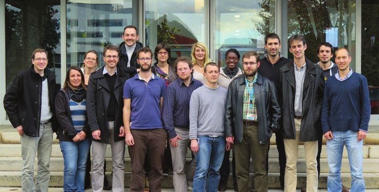
Lux Aixala, Violaine Salvador, Julia Simon, Gilles Gaillard, Guillaume Savelli, Mathieu Boidot, Christelle Navone, Valérian Cinçon, Alizee Visconti,
Jean Leforestier, Magatte Gueye, Jesus Carrete Montana, Alexandre Carella, Thierry Baffie, Etienne Yvenou, Sébastien Vesin.
Thermoactive materials appear as a new class of materials in the field of new technologies for energy mainly addressing
the domain of energy harvesting. Thermoelectric generators (TEG) are designed for benefiting from waste heat to produce
electricity often with a limited power output. Nevertheless, it permits to increase the overall efficiency of systems where
the competing technologies cannot be used.
Combining N-type and P-type thermoelectric (TE) materials, TEG directly convert temperature differences to electric
voltage with an efficiency related to the dimensionless figure of merit ZT, which is defined by:
(Eq.1) ZT=(σ×S²)/λ T
where σ, S, λ and T are the electrical conductivity, the Seebeck coefficient, the thermal conductivity and the temperature,
respectively. The higher the ZT value, the better the thermoelectric behavior. ZT values are spread around 1 depending on
the nature of the materials and the temperature range. Moreover, as shown in Equation 1, performances of TE materials
strongly depend on the temperature range of desired applications.
1 - THEORETICAL APPROACH: FROM VALIDATION TO PREDICTION
Thanks to our development of a novel method to predict materials thermal conductivity from first principles1, we have
been able to perform the first high throughput investigations of thermoelectric materials. So far we have investigated the
wide class of materials known as half Heuslers. From 79,057 theoretical compound entries, we found 75 stable compounds
(figure 1).
Our team is also recognized for pioneering and advancing the field of thermal conductivity calculations from first principles.
We have recently demonstrated that it is possible to achieve crystalline SiGe nanostructures with thermal conductivities
much lower than the so called “alloy limit”.
We are also the creators of computer program “ShengBTE” www.shengBTE.org published in 2014. This is the first publicly
available software capable of predicting thermal conductivity of crystalline materials from first principles, and it has a
growing community of users.
8
Fig. 1 - Number of
                                                                                                                                                 compounds during the
                                                                                                                                                 screening (left) and
                                                                                                                                                 evolution of the valence
                                                                                                                                                 per unit cell distribution
                                                                                                                                                 (center). All the final
                                                                                                                                                 75 compounds follow
                                                                                                                                                 the 8/18 octet rule.
                                                                                                                                                 Distribution of nano-
                                                                                                                                                 grained ZT at different
                                                                                                                                                 temperatures for the
                                                                                                                                                 stable half-Heuslers,
                                                                                                                                                 compared to standard
                                                                                                                                                 semiconductors2 (right).

2 - NANOSTRUCTURATION OF MATERIALS
2.1 - NANOSTRUCTURATION WITHIN BULK MATERIALS

As compared to a monolithic material, theoretical calculations have shown that a small volume fraction of a nanometer-
size second phase, homogeneously dispersed in the microstructure of a sintered polycrystalline material, leads to a
drastic reduction of the lattice thermal conductivity without affecting the power factor3. Then a strong increase of the ZT
parameter is predicted. Dense n type Mg2Si0.5875Sn0.4Sb0.01254 and p type MnSi1.775 polycrystalline alloys (grain size of 7 and
10 μm, respectively) have been prepared by gas-phase atomization followed by spark plasma sintering. Both materials,
devoted to applications in the range 200-500 °C, have been nanostructured by tailoring an intensive in-situ precipitation
during the sintering step (no second phase added). The formed precipitates have a nanometer-size character (average
diameter ranging from 7 to 20 nm and concentrations around 5.1x10⁻³ and 8.9x10⁻⁴ /nm2 for the Mg2Si0.5875Sn0.4Sb0.0125 and
MnSi1.77 alloys, respectively) (Figure 2).

 Fig. 2 - left a) N-type Mg2Si0.5875Sn0.4Sb0.0125, b center) P-type MnSi1.77, c right) ZT parameter as function of temperature compared to the State-of-art (SOA).

As shown in Figure 2, high ZT values are obtained that are among the best reported for this kind of materials. Similar
trends have been observed on N and P-type Si92Ge086 alloys that have been nanostructured ex-situ (a second phase is
incorporated).

2.2 - NANOSTRUCTURATION WITHIN THIN FILMS

The research on thermoelectric systems based on thin films is mainly driven by applications in the microelectronic field
where the energy consumption due to heat losses in large computers becomes a crucial problem. For ten years we have
developed materials compatible with microelectronic applications. Silicon- and germanium-based materials have been
chosen as TE active materials. Thus Si/SiGe superlattices, then SiGe/Ge quantum dots superlattices (n- and p-doped, mono-
and polycrystalline, for both cases) have been grown by using an industrial Reduced Pressure CVD tool, highlighting a
decrease of the thermal conductivity compared to bulk materials7-8.

                                                                                                                                                                              9
More recently, new kind of SiGe-based nanostructures have been grown based on our theoretical works that suggested
     the use of silicides as competitive TE9. For the first time, n- and p-doped, mono and-polycrystalline, silicide quantum dots
     superlattices have been grown. These new nanostructures integrate TiSi2 or MoSi2 dots in a SiGe matrix, as illustrated in
     figure 3. The TE characterization of these nanostructures has shown a simultaneous increase of the in-plane power factor
     by a factor 3.5 thanks to the modulation of the doping effect and a decrease of the cross-plane thermal conductivity down
     to 20 %, by adding phonon diffusion by the dispersion of nanoparticles at 300 K10-11-12.
     The perspectives consist in integrating our new nanostructured materials in thermoelectric generators. To reach this goal,
     a thesis has started at the beginning of 2015 on this topic, in partnership with the Université de Sherbrooke, Canada, and
     an ICT25 European project (STREAMS) will start at the beginning of 2016.

                                                                         (a)                                              (b)

     Fig. 3 - Cross section TEM images ofn-SiGe/TiSi2 mono- (a) and polycrystalline (b) quantum dots superlattices.

     3 - FROM MATERIALS TO ASSEMBLY AND SYSTEMS

     The applications require the assembly of many TE legs together within a TE module, which can stand long time in harsh
     operating conditions. For energy saving applications, a high cadency production of TE modules is needed, since every
     module is only delivering few watts. Current approach is a planar assembly of legs between electrodes. The challenge at
     this step is to deliver a strong and reliable assembly technology which offers a minimum electrical resistance. Moreover,
     it is important to reduce chemical diffusion between TE material and surrounding elements. The thermal coefficient
     mismatch should be minimized13. A novel assembly technology based on nano-silver soldering has been investigated,
     with promising results. More than 1000 cycles (150 °C-400 °C) and 500 h durability testing (550 °C) have been successfully
     achieved with minor power output reduction14 . Technological solutions are under investigation to prevent the oxidation
     which was identified as the main failure mode of our devices.
     Thermoelectric modules are further integrated in thermoelectric generators (TEG) which may comprise single module or
     multiple modules. Maximum output power of such system is today limited to tens of kW15-16 and requires a huge number
     of TE modules since overall efficiency remains limited, below 10 %. TEG prototypes using Bi2Te3 and Si80Ge20 thermoelectric
     modules were simulated (under Matlab®), prototyped, assembled, and tested at CEA17. Output power reached from 30 W
     to 100 W as a function of inlet gas temperature varying from 450 °C to 750 °C (figure 4). Further improvement potentials
     were identified. A 1 kW prototype of TEG based on Bi2Te3 dedicated to marine engines has been built by HotBlock OnBoard,
     our industrial partner, with the support of CEA, and will be used as a communication product during 2015.
     Further research activities are ongoing with Valeo and HotBlock OnBoard through the “RENOTER2” funded project. CEA
     is manufacturing “net shape” sustainable and low cost TE materials Mg2Si0,4Sn0,6 and MnSi1,77 for automotive applications
     (figure 5). Such exhaust heat exchanger for hybrid gasoline vehicles may be able to reach a maximum power output of 240
     W leading to 4 g/km of CO2 emission reduction.

10
Fig. 4 - 45W thermoelectric generator using 30 Si80Ge20 TE modules. Fig. 5 - TE ring manufactured by CEA and their assembly in a
TE tube generator by Valeo
ORGANIC THERMOELECTRICITY ORGANIC THERMOELECTRICITY
For low temperature thermoelectric materials (T < 200 °C), electrical conductivity. Highly conductive polyaniline
the record is still being ZT=1.2 at room temperature and poly(3,4-ethylenedioxythiophene (PEDOT) are
(ZT=1.5 at T=100 °C) for bismuth telluride alloys. But the prepared thanks to patented CEA procedures18. PEDOT
mass implementation of TEG based on bismuth telluride stabilized with trifluoromethane sulfonate exhibits a
is prevented by a high production cost. Since 2011, we very high conductivity above 1200 S/cm. Treatment
have been exploring the use of polymers and composites with sulfuric acid improves electrical conductivity above
for low temperature TE applications. These materials 2200 S/cm thanks to a better crystallinity and the highest
exhibit a very low thermal conductivity (typically 0.2 reported oxidation state for PEDOT materials19. The
– 0.4 W/K) hence our efforts are mainly focused on the Seebeck coefficient of PEDOT can be increased from 18
increase of both the Seebeck coefficient and the μV/K up to 160 μV/K thanks to the fine redox control of
the charge carrier concentration. This treatment leads to
PEDOT materials with ZT above 0.1 which is among the
best reported values20. Innovative processing methods
have been developed to obtain free standing films of
PEDOT and their easy transfer on various substrates
without affecting their thermoelectric properties, even
for thick layers. n-type TE materials based on coordination
polymers (poly[Kx(Ni-1,1,2,2-ethenetetrathiolate)]) have
been formulated and processed in combination with
PEDOT materials in TE devices such as efficient flexible
heat flux sensors.
2D heat flux sensors producing 5mV from the body heat
1 - W. Li, J. Carrete, N. A. Katcho, N. Mingo, Computer Physics Communications 185 (6), 1747-1758 (2014)
2 - J. Carrete, Wu Li, N. Mingo, S. Wang, S. Curtarolo, Physical Review X, 4, 011019 (2014) 11 - G. Savelli et al., Nanotechnology 26, (2015)
3 - N. Mingo et al. : Nano Lett, 9, 711, (2009) 12 - G. Savelli et al., Thin Solid Films, accepted, (2015)
4 - G. Bernard-Granger et al. : submitted to Acta Materialia, (2014) 13 - M. Schwartz : Brazing – 2nd edition – ASM International (2003)
5 - G. Bernard-Granger et al. : J Alloys Comp, 618, 403, (2015) 14 - L. Aixala et al. : presentation at IAV 4th thermoelectric congress, Berlin, Germany, (2014)
6 - K. Favier et al. : Acta Materiala, 64, 429, (2014) 15 - Alphabet Energy : http://www.prweb.com/releases/2014/10/prweb12229734.htm
7 - G. Savelli & al., J. Micromech. Microeng. 18, (2008) 16 - H. Kaibe et al. : http://www.komatsu.com.sg/CompanyInfo/profile/report/pdf/164-E-05.pdf (2011)
8 - D. Hauser & al., Thin solid Films 520, (2012) 17 - K. Romanjek et al. : submitted to Journal of Electronic Materials (2014)
9 - N. Mingo & al., Nano Lett. 9, (2009) 18 - A. Carella & al, Patent pending, (2014)
10 - S. Silveira Stein & al., Proc. IEEE Nano Conf., Toronto, Canada, (2014) 19 - N. Massonnet & al, Chem. Sci., (2015)
20 - Q. Zhang & al, Adv. Mater., (2014)
11Synthesis and purification of copper nanowires
for flexible transparent electrodes
CONTEXT to tackle potential issues such as stability and scale-up of the che-
Transparent conductive thin films are essential components for mical synthesis of the nanowires. Studies are ongoing.
touch screens, solar cells and many other optoelectronic devices.
The fabrication of transparent electrodes is commonly realized PARTNERS, FUNDINGS, ACKNOWLEDGMENTS
with indium tin oxide (ITO). However, ITO is not able to meet the This work benefited from a grant by the DGA (Direction Générale
future demands for flexible transparent conductive films in parti- de l’Armement).
cular because of its intrinsic brittleness.
APPROACH
References
Great efforts have been devoted to develop new materials pro-
[1] Langley D., Giusti G. Mayousse C., Celle C., Bellet D., Simonato J.P.,
duced at low cost, and processable at low temperature. Among Nanotechnology, 2013, 24, 452001
them metallic nanowires used in the form of random networks [2] Mayousse C., Celle C., Fraczkiewicz A., Simonato J.P., Nanoscale,
appear as a very promising alternative to ITO. Though mainly silver 2015, 7, 2107-2115
has been used so far [1,2], the use of less expensive metals such as [3] Mayousse C., Celle C., Carella A., Simonato J.P., Nano Research,
copper would certainly be of interest [3]. 2014, 7(3), 315-324
RESULTS
The hydrothermal synthesis of long copper nanowires (up to hun-
dreds of microns) has been demonstrated. It is based on a simple
protocol using only water, copper chloride and octadecylamine
which play both the roles of reducing and capping agents (the lat-
ter is necessary to promote a one-dimensional growth). We have
also shown that the purification of the nanowires is very impor-
tant and can be easily achieved by wet treatment with glacial ace-
tic acid. The process is carried out at room temperature and no
post-treatment is necessary.
Fabrication of random networks of purified copper nanowires
leads to highly flexible transparent electrodes with excellent Fig. 1:Transmittance as a function of the sheet resistance for Cu
optoelectronic performances (e.g., 55 Ω/ at 94% transparency, nanowire based electrodes
Inset: Cu nanowires deposited on a flexible PEN substrate
Figure 1). Like for silver nanowires based electrodes a high trans-
parency in the mid-infrared region was measured.
Both transparent conductive materials were successfully inte-
grated in capacitive touch sensors to demonstrate a potential
application of these nanowires based flexible transparent electro-
des. Briefly, when a conductive object such as a finger is approa-
No contact
ching or touching the electrode through the protective coating,
the local electric field is modified and induces a capacitance
change, which can be monitored and used to modulate for ins-
tance the lighting power of a LED (Figure 2). The touch sensors
were functional for at least several months.
Contact
In addition, hybrid materials with the conductive polymer PEDOT:
PSS show similar properties (e.g., 46 Ω/ at 93% transparency), Fig. 2: Use of Cu NW based electrodes on a capacitive touch sen-
with improved mechanical properties. sor. The capacitance change is operated by approaching a finger
close to the surface, which modifies oscillation values (top 362;
down: 273)
CONCLUSIONS AND PERSPECTIVES
The performances obtained with these copper nanowires are very TEAM
good and meet the requirements of many applications, in particu- Céline Mayousse, Caroline Celle, Alexandre Carella,
lar for optoelectronics. Further studies are nonetheless expected Jean-Pierre Simonato .
CONTACT
jean-pierre.simonato@cea.fr , caroline.celle@cea.fr
12Doping efficiency of single and randomly stacked
bilayer graphene by iodine adsorption
CONTEXT PARTNERS, FUNDINGS, ACKNOWLEDGMENTS
To produce large scale transparent conductive electrodes based This work was carried out in the frame of the GraphEN collabora-
on bi dimensional graphene material, conductivity enhancement tive project between Liten, Leti, Inac and Neel Institute.
through efficient doping is needed. Indeed while graphene exhi-
bits a very high carrier mobility in theory, it suffers from a rather
low carrier density. Thus the carrier density has to be enhanced
by doping to produce transparent conducting film and fulfill the
specifications requested by the applications (Transmission >90%
with square resistance below 100 Ohm). Unlike dopant chemi-
sorption, dopant physisorption appears especially promising as it
can increase the charge carrier concentration and maintain a high
level of carrier mobility. References
[1] Kim, H., Renault, O., Tyurnina, A., Simonato, J.P., Rouchon, D.,
APPROACH Mariolle, D., Chevalier, N., Dijon, J.
Among the wide variety of dopants that can be physisorbed on Doping efficiency of single and randomly stacked bilayer graphene
by iodine adsorption
graphene one of the most promising is iodine. The graphene
(2014) APPLIED PHYSICS LETTERS Volume: 105 Published: JUL 7 2014
doping of type p (holes) by iodine vapor at relatively low tempe-
rature (100 °C) is suitable for significantly improving the conduc-
tivity of graphene and carbon nanotubes. CVD grown graphene
samples have been prepared on platinum at rather low tempe-
rature (700°C) and transferred on Si/SiO2 substrate by electro-
chemistry using bubbling of hydrogen at the interface between
Pt and graphene. These samples where used to make electrical
characterization and X-ray photoelectron emission microscopy
(XPEEM) to assess the doping efficiency and stability on single
layer or folded double layer graphene (figure 1).
RESULTS Fig. 1 - left: energy filtered secondary electron PEEM image and
work function map (right) of 1L and 2L doped graphene layer
Polyiodide complexes (I3- and I5-) have been identified by XPS and
Raman spectroscopy as the doping species. The graphene work
function increases from 4.3eV to 4.7 eV after iodine treatment
(figure 2). More efficient doping has been observed on the bilayer
thanks to iodine complexe intercalation. The amount of iodine on
the surface is close to 1% and very interestingly the doping effi-
ciency is maintained up to 300°C but with a slight decrease for
temperature larger than 200°C (figure 2). These results have been
confirmed by electrical measurements on devices revealing a
resistivity decrease from 2 kOhm square down to 670 Ohm square
after iodine doping.
CONCLUSIONS AND PERSPECTIVES
The efficiency of iodine as a p type dopant up to 300°C on CVD
graphene has been demonstrated. Bilayer graphene was found to Fig. 2: Work function and iodine concentration evolution versus
annealing temperature.
contain a higher amount of dopant than single layer graphene,
suggesting that iodine can intercalate between the layers of the
non-Bernal stacked graphene which is not the case for graphite.
These preliminary results open new perspectives for stable TCF TEAM
based on doped stacked graphene layers. Anastasia Tiurnina, Jean Dijon, Jean-Pierre Simonato,
Olivier Renault, Hokwon Kim
CONTACT
jean.dijon@cea.fr , jean-pierre.simonato@cea.fr;
olivier.renault@cea.fr 13Photonic Nanojet: a promising fabrication tool
for producing functionalized surfaces
CONTEXT
High density periodic nanostructures over very large surfaces (>> PARTNERS, FUNDINGS, ACKNOWLEDGMENTS
cm²) are very promising in the domain of energy for example to Laboratoire Hubert Curien, Prof. Yves Jourlin, St Etienne.
optimize solar cells efficiency, reduce engine friction, minimize
aircraft drag, enhance electrical systems lifetime by improving References
polymer surface hydrophobicity. However, very few lithography [1] O. Delléa et al., IPAS 2014, Springer, Berlin Heidelberg, 107–117.
techniques fulfill all the required criteria: spatial resolution, low [2] O. Delléa, O. Shavdina et al., submitted patent, n°15 52837.
writing time, low cost, compatibility with a wide range of materials [3] O. Shavdina, O. Delléa et al., Langmuir 2015, 31, 7877−7884.
or non-planar surfaces.
APPROACH
Nanosphere lithography, also called colloidal lithography, based
on the assembly of size-monodisperse nanospheres is an easy,
inexpensive, efficient, and flexible manufacturing approach[1].
Usually, the 2D hexagonal closed packed nanoparticle array is
used as mask. Our approach consists in using the focalizing pro-
perties of the spheres to pattern the substrate. Indeed, being irra-
diated by an optical beam, each sphere is acting as a near-field
microlens generating a field enhancement underneath, called
“photonic nanojet”.
Fig. 1: Electric field
in symmetry plane
RESULTS of the spheres of
We first applied the rigorous coupled wave analysis (RCWA) theory 1µm.
to calculate the electric field distribution during the illumination
of a microsphere hexagonal 2D array with a plane wave (fig. 1).
We observed that nanojets can be generated for a wide range of
microsphere diameters (from 2λ to more than 40λ) and investi-
gated key parameters to optimize the energy, focus, diameter and
length of the nanojets (fig. 2) [2]. We demonstrated for example the
Fig. 2: Optimized
possibility to increase both the energy and the focus of the nano- calculation of
jet by a factor greater than 2. nanojet parameters
Depending on the operating conditions and the nature of the in comparison with
conventional nanos-
substrate on which the particles are deposited, the photonic phere assembly.
nanojet can achieve the following physical operations: ablation,
crosslinking, photolysis, growth of metallic nanoparticles, fusion.
Experimentally, an enhanced Langmuir Blodgett technique
called Boostream® compatible with 2D or 3D large surfaces [3] was
employed to transfer 1 µm silica sphere arrays on photosensitive
TiO2 xerogel previously deposited on glass. The insolation and
development condition has lead to a large area hexagonal array
of periodically organized nanopillars (fig. 3) in accordance with
theory. Fig. 3: Large area
hexagonal array of
periodically orga-
CONCLUSIONS AND PERSPECTIVES nized TiO2 nanopillars
Photonic nanojet is a maskless subwavelength-resolution direct
write nanopatterning tool combining several physical pheno-
mena at subwavelength scale. Our future work will focus on the
fabrication and characterization of smart surfaces associating TEAM
periodic structures and nanoparticles growth for catalysis. Olivier Delléa, Olga Shavdina, Pascal Fugier.
CONTACT
olivier.dellea@cea.fr
14Twisting phonons in complex crystals with
quasi-one-dimensional substructures
CONTEXT PARTNERS, FUNDINGS, ACKNOWLEDGMENTS
A variety of crystals contain quasi-one-dimensional (1D) substruc- This work has emerged from a consortium including the theory
tures, which yield distinctive electronic, spintronic, optical, and team at Liten/DTNM and several other world-leading theoretical
thermoelectric properties. There is a lack of understanding of the and experimental groups at Oak Ridge National Lab, Cornell Uni-
lattice dynamics that influences the properties of such complex versity and the University of Texas, among others. The full list of
crystals. participants and further details can be found in[1]. This work was
partly carried out in the frame of two projects : PHIMS (ANR) and
APPROACH SIEVE (CARNOT).
Here we employ inelastic neutron scatting measurements and
density functional theory calculations to show that numerous
low-energy optical vibration modes are present in higher man-
ganese silicides (HMS), an example of such crystals. Including unu- References
[1] Chen et al.,
sually low-frequency twisting motions of the Si ladders inside the
Nature Communications, 6 :6723 (2015)
Mn chimneys, these optical modes provide a large phase space
for scattering acoustic phonons. A hybrid phonon and diffusion
model is proposed to explain the low and anisotropic thermal
conductivity of HMS and evaluate nanostructuring as an approach
to further suppressing the thermal conductivity and enhancing
the thermoelectric energy conversion efficiency.
RESULTS
These experiments and calculations clearly reveal that the complex
Nowotny chimney ladder structure of HMS gives rise to numerous
low-lying optical vibration modes, including a peculiar twisting
polarization that undergoes avoided crossings with the acoustic
branches near the Brillouin zone center. In addition, the calcula-
tion reveals a reversal of the group velocity anisotropy at energies
above and below about 10 meV. These observations help explain
the considerable anisotropy in the thermal conductivity of HMS.
According to a combined low-frequency phonon and high-fre-
quency diffusion model, our calculation suggests that glass-like
thermal conductivity is achievable by introducing grain boundary
scattering with a length scale of about 10 nm. Therefore, a ZT lar-
ger than 1 is possible by nanostructuring HMS, as a ZT of 0.6-0.7
has been achieved in doped samples with grain size of several
micrometers. More broadly, the twisting polarization discovered
in HMS gives the first glimpse of the elusive and important lattice
dynamics in a wide range of complex crystals with promising func-
tionalities as a result of internal quasi-1D substructures.
CONCLUSIONS AND PERSPECTIVES Fig. 1: Measured INS (ARCS) signal and simulated dynamical
This discovery offers new insights into the structure-property rela- structure factor for the HMS crystal at 300 K. S(Q,E) data obtained
tionships of a broad class of materials with quasi-1D substructures by ARCS (top) for the HMS crystal and simulated dynamical struc-
ture factor (bottom) for Mn4Si7, a, along [H00] in the (4,0,0) Bril-
for various applications. louin zone, showing the LA and LO modes
TEAM
Natalio Mingo, Jesus Carrete Montana.
CONTACT
natalio.mingo@cea.fr , jesus.carretemontana@cea.fr
15Integration of a graphene ink as gate electrode for
printed organic thin-film transistors
CONTEXT
Great progress has been made in the development of organic
electronic materials since the discovery of conducting and semi-
References
conducting polymers. These materials can be processed in solu- [1] M. Benwadih et al. / Organic Electronics 15 (2014) 614–621
tion, as inks. Traditional high-volume printing techniques can be
used for manufacturing of organic electronic devices on various
flexible substrates at low cost. The development of solution of
organic semiconductors has allowed the emergence of a new
generation of air-stable P- and N-type materials for Organic Thin-
Film Transistors (OTFTs).
APPROACH
CEA Liten proposed to integrate a graphene ink as gate electrode
in a printed complementary organic technology, which exhibits
performance and process compatibility that complies with low
cost objectives.
RESULTS
Complementary printed OTFTs have been manufactured with Fig. 1: Comparison of transfer characteristics of P-type (left) and N-type (right)
graphene ink as a gate electrode allowing obtaining higher semi- OTFTs with a 500 nm- and 750 nm-thick dielectric
conductor mobilities : 3 cm2V-1s-1 for the P-type and 0.9 cm2V-1s-
1
for the N-type have been achieved (figure 1). The seven-stage
ring oscillator has reached high oscillation frequencies of 2.1 kHz
at 40 V, corresponding to a delay/gate value of 34 µs (figure 2).
The use of 1% wgt adhesive in the silver paste is mandatory to
have a good adhesion on the CYTOP dielectric layer. However it
decreases the gate dielectric capacitance and consequently the
electrical performance of the transistors. The use of graphene ink Fig. 2: Output charac-
as a gate in the organic complementary technology has enabled teristics of an organic
seven-stage ring
a lower cost and a higher electrical mobility than the silver paste oscillator (L =20 µm
(figure 3). Different morphological and electrical characterizations W =1000 µm) with
Vdd = 20 V
have been conducted on the graphene ink to optimize its integra-
tion in organic devices. A value of 37 Ω/sq was measured for the
sheet resistance of the printed graphene ink, the roughness of the
layer characterized by AFM was 78 nm. Besides, the decrease of
dielectric thickness has lowered the threshold voltage around 10
V, which was the goal to reach in order to use lower supply vol-
tages (15 V).
CONCLUSIONS AND PERSPECTIVES
This process may give rise to other kinds of new and highly rele-
vant techniques combining altogether very high performances, Fig. 3: Picture of an
reliability and low fabrication costs. organic circuit on
flexible substrate
PARTNERS, FUNDINGS, ACKNOWLEDGMENTS
This work was funded in the frame of the European FP7 project
COSMIC. The authors want to thank Polyera Corp. for supplying
N-type semiconductor ActivInk® material. TEAM
Mohammed Benwadih, Abdelkader Aliane,
Jacqueline Bablet
CONTACT
mohammed.benwadih@cea.fr
16EQE asymmetry and capacitance depletion in semi-transparent
organic photodetector: characterization and modeling
CONTEXT
Semi-transparent bulk heterojunction organic photodiodes pro- References
cessed in air present singular features. Depending on the cha- [1] B. Bouthinon, R. Clerc, J.M Verilhac, S. Jacob, A. Gras, J. Joimel, O.
racteristics of the active layer (polymer energy level, active layer Dhez, A. Revaux,
thickness …), the External Quantum Efficiency (EQE) can show ICOE 2014
significant differences when the device is illuminated either from
the substrate side or from the top side [1]. These differences are
independent of the optical absorption of the stack. This work aims Fig. 1: Schematic of organic photodetector investi-
at understanding the causes of this unknown internal dissymme- gated in this work.
try.
APPROACH
To investigate this issue, photodiodes presenting the typical
inverted architecture shown in Fig. 1 are processed and investi-
gated for different blend thicknesses. EQE from both sides (fig.2)
and Capacitance versus Voltage characteristics (fig.3) have been
measured and compared to TCAD (Technology Computer Aided
Design) simulation.
RESULTS
Results shown in Fig. 2 indicate a large discrepancy between
back and front EQE, the back side being 3 times more efficient Fig. 2: Experimental back and front side External
than the front side at 0V and 620 nm. This discrepancy is reduced Quantum Efficiency (EQE) measured at 0V.
when increasing the reverse polarization. When such a diffe-
rence appears, a depletion zone of about 200 nm (thinner than
the active layer in the case of photodiodes) is extracted from the
complementary capacitance versus voltage measurement in the
dark (Fig. 3). These two features (EQE asymmetry and capacitance
depletion) are the signature of charged species present in the
active layer gap. These charges lead to potential bending (Fig.
Fig. 3: Capacitance – voltage
4) and apparition of a low electric field zone close to PEDOT: PSS characteristics measured
electrode. TCAD simulation allows reproduction of all photodiode (dots) and simulated (lines) in
dark condition at a frequency
experimental characteristics either using p-type doping (which response of 100Hz before and
would be unintentional in our case) or by including acceptor after ageing.
states. The amount of species increases after ageing and leads to
higher depletion (Fig.3) and EQE dissymmetry.
CONCLUSIONS AND PERSPECTIVES
The presence of charge species in the gap of organic photodiode
active layer layer leads to high. It leads to high dissymmetry
between front and back performance of the device. This pheno- Fig.4: Simulated potential in
menon is amplified after ageing of the device. Next step will be to the active layer at 0V under
illumination showing the
determine the origin of these gap states. impact of the acceptor like
trap state on the potential
PARTNERSHIP distribution.
This work was performed in partnership with the start-up ISORG.
CONTACT
amelie.revaux@cea.fr
17Printed microsensors arrays for monitoring of batteries and
fuel cells
CONTEXT CONCLUSIONS AND PERSPECTIVES
Accurate monitoring of electrochemical generators such as batte- Printing technology demonstrated the capability to produce
ries and fuel cells is necessary to optimize performance and dura- non-intrusive arrays of micro sensors that could be placed directly
bility in addition to increase safety. For that purpose, more and on batteries or in fuel cell to record numerous different relevant
more information from the individual cells under operation are parameters for in-operando monitoring. This low cost process can
required (temperature and cell voltage distribution, mechanical be used to drastically reduce the cost of the instrumented cells.
stress, deformation…). Operando monitoring of the cells thanks It remains, however, to develop the tools that could analyse and
to low cost and minimally invasive sensors is thus necessary. integrate all these information into the generator’s management
system.
APPROACH
Arrays of micro-sensors were produced using printing as low cost PARTNERS, FUNDINGS, ACKNOWLEDGMENTS
process of fabrication. For battery monitoring, arrays of sensors This work was partly carried out in the frame of a national program
composed of three types of sensors were developed: temperature Institut Carnot Energy for Future (MICROCAPT).
sensors (Wheatstone bridges, using positive temperature coeffi-
cient and negative temperature coefficient materials inks), polyvi-
nylidene difluoride (PVDF) piezoelectric sensors for acoustic emis- References
[1] N. Kircheva, PhD thesis, INPG, Grenoble, 2013
sion [1,2], and strain gauges [3]. [2] S. Genies et al. Patent EP2702632 A1, 2011
For fuel cell (PEMFC) application, the objectives were notably to [3] STALLION Project ref: 308800,FP7-ENERGY-2012
produce arrays of sensors for the mapping of local voltages. These [4] A.G. Hsieh et al Energy Environ. Sci., 2015,8, 1569-1577
sensors had to be directly placed in the cell, either between the
gas diffusion layer (GDL) and the bipolar plate (BP) or integrated
inside a Membrane/ Electrode Assembly (MEA).
The micro-sensors arrays were printed on flexible support such as
a polymer or a paper sheet or directly on the sample to monitor.
RESULTS
Arrays of sensors used for battery application demonstrated the Fig. 1: Evolution of
the temperature
possibility to record the temperature variation and the gradient of recorded by six
temperature that appears on a cylindrical 18650 battery between printed sensors
the ends of the cylinder (connectors) and the middle (Fig. 1) (Wheatstone bridge)
placed on a 18650
during cycling. PVDF piezoelectric sensors were used to detect the battery during
acoustic signals emitted by Li-ion batteries during operation. In discharge (1C rate).
particular, it was possible to detect the early signs of the thermal
runaway and prevent fire or explosion of the battery issued from
over-heating (Fig. 2). Piezo sensors were also used for preliminary
tests of ultrasound characterization as initiated by [4].
Preliminary tests were also conducted on strain gauges directly
printed on pouch cells package. Fig. 2: Principle of
For PEMFC, arrays of microsensors were printed on Polyethylene ultrasonic acoustic
characterization
terephthalate (PET) and Polyether ether ketone (PEEK). The ther- using printed PVDF
momechanical behaviour of the PET (Tg≈100°C) has allowed a piezoelectric sensors
successful integration of a first one inside a MEA (Cf. top figure at for batteries study.
Example of use of
the middle) while a second one has been cut in order to design an piezo sensors for the
open instrumented grid to probe local voltages between bipolar detection of early
plates and MEA into stacks. Both are currently being validated in signs of the thermal
runaway of a battery
fuel cells.
TEAM
Nicolas Guillet, Romain Gwoziecki, Jean Francois Blachot
CONTACT
nicolas.guillet@cea.fr
18Vous pouvez aussi lire