RECHERCHE HEPL CAMPUS - NOS JEUNES ONT DU TALENT ! - Pour toutes informations HEPL Cellule REPROFOR
←
→
Transcription du contenu de la page
Si votre navigateur ne rend pas la page correctement, lisez s'il vous plaît le contenu de la page ci-dessous

RECHERCHE HEPL
 CAMPUS
 S C I EN C ES E T T E C H N I Q U E S
 NOS JEUNES ONT DU TALENT !

Pour toutes informations

HEPL Cellule REPROFOR
cellule.recherche@hepl.be

 RECHERCHE HEPL VOLUME 1 | 2022

TABLE DES
MATIERES

01
L’EDITO

02
Journée des Chercheurs en HE L’EDITO

 La HEPL offre aux étudiantes et étudiants de Sciences

 et Techniques ainsi qu’aux jeunes chercheurs des
 Chers lecteurs, occasions uniques et stimulantes de se familiariser

 avec la recherche tout en réfléchissant à leurs
 La recherche en Haute École est résolument tournée
 orientations et à leurs objectifs professionnel.
 vers la résolution de problèmes pratiques et

 appliqués au bénéfice de la société civile ou des

 entreprises. Ce magazine est une occasion en or pour leur permettre de

 12 Elle fédère les forces vives de la HEPL

 de projets innovants et passionnants contribuant à
 autour partager avec vous le fruit de leur travail.

 Je vous en souhaite bonne lecture.
 Travaux d’étudiants – Master 2 développer l'expertise des enseignants et des
 électronique
 étudiants.

 26 Nathalie Gerlach

 Editrice, Recherche HEPL

 Travaux d’étudiants – 2ème Bachelier
Get a freeconsultation by checking out www.lolafurniture.com

 CAREMAN
JCHE 2022 Cette année, la section Sciences et Techniques
 .

 a été dignement représentée à ce colloque par

La Journée des Chercheurs en Haute École le biais d’une présentation poster intitulée

(JdCHE) est un colloque scientifique annuel Différents types de projets peuvent ainsi être mis « Projet PuMA » effectuée par notre chercheuse

organisé par SynHERA. Cet événement se veut en valeur, qu’ils portent sur des recherches en Elodie Jamotton et par la publication d’un acte Elodie Jamotton est chercheuse sur le projet

être une véritable vitrine de la recherche démarrage ou en cours, sur une méthode ou un de colloque portant sur le projet INDTHERM et WIN²WAL PuMA (PhotocondUctance Multiscan

appliquée réalisée par les Hautes Écoles et leurs processus innovant. rédigé par notre chercheur Arnaud Cawez, en system for Advanced substrate). Elodie a un

Centres de Recherche associés dans différentes collaboration avec Denis Helsen, chercheur à Masters en ingénieur civil biomédical avec une

thématiques. De plus, cette journée donne l’opportunité aux l’IRISIB, partenaire du projet. spécialisation en électronique .

 chercheurs de se rencontrer, d’échanger, de

La JdCHE permet aux chercheurs débutants ou s’inspirer mutuellement, et de découvrir la Tout cela n’aurait pas été possible sans

confirmés de présenter leurs travaux de recherche richesse de l’écosystème de la recherche l’encadrement efficace et motivant de

au travers des communications orales ou des appliquée en Haute Ecole. Christophe Brose, chef du projet PuMA et

présentations posters. Philippe Demy, chef du projet INDTHERM !
 Arnaud Cawez est chercheur sur le projet

 WIN²WAL INDTHERM. Arnaud a un Master en

 ingénieur civil aérospatial et arbitre de basketball
 2 | RECHERCHE HEPL | 2022
 durant ses temps libres.
 | 5

Conception d’un système de caractérisation sans contact des substrats hautement résistifs

 Projet PuMA

JAMOTTON Elodie1 (elodie.jamotton@hepl.be) ; SCHEEN Gilles2, 3 ; BROUN Valéry2 ; BROSE Christophe2

1 CeCoTePe, Seraing, Belgique

2 Haute Ecole de la Province de Liège, Département ingénieur, Liège, Belgique

3 Incize, Louvain-la-Neuve, Belgique

Mots-clés : caractérisation, sans contact, Trap-Rich High Resistivity Silicon-On-Insulator (TR HR SOI), semi-conducteur, Internet of Things

La technologie RF-SOI (Radio Frequency Silicon-on-Insulator) prend beaucoup d’importance à ce jour grâce à ses caractéristiques fortement

adaptées aux applications sans fil. Actuellement, la plupart des circuits commutateurs d’antenne sont fabriqués sur des tranches de RF-SOI,

souvent appelées « substrats ». En effet, ces substrats concernent tout le marché de la téléphonie mobile en 3G et en 4G ainsi que le marché

des tablettes et bientôt le marché de l’IoT (Internet of Things)4. Cependant, une bonne communication sans fil dépend de la qualité du

groupe de circuits qui reçoit le signal venant de l’antenne. Il faut donc que ce groupe de circuits soit capable de traiter le signal entrant et le

signal sortant avec la meilleure performance en ce qui concerne l’isolation entre les différents signaux ; les pertes dans les signaux entrants

ou sortants ; et surtout la linéarité du signal.

Avec l’avènement de la 5G, les performances de la technologie RF-SOI ne suffisent plus et celle-ci s’est vue améliorée en technologie « Trap-

Rich High Resistivity SOI »2, 3 (TR HR SOI). Dans cette technologie, une couche de passivation enrichie de pièges est introduite entre l’oxyde

enterré et la base de silicium hautement résistif. Cette nouvelle couche a pour rôle de limiter les charges mobiles qui s’accumulent à l’interface

entre l’oxyde et le silicium car ces charges réduisent fortement la qualité de la tranche RF-SOI dans les applications haute puissance et haute

fréquence.

Avant de placer les circuits électroniques sur les substrats, il est nécessaire de vérifier qu’ils ont bien les performances attendues. A ce jour,

la seule manière de procéder est de réaliser un test destructif sur des tranches choisies, parmi le lot de substrats, comme échantillons de

test. Ces tranches ne sont donc plus utilisables ensuite. Cette méthode pose différents problèmes : seules certaines tranches sont testées

dans un lot ce qui n’assure pas la qualité de toutes ; la réalisation des tranches de TR HR SOI est plus coûteuse que les anciennes technologies

ce qui augmente grandement le coût des tests ; les ressources utilisées pour la création des substrats sont de plus en plus rares et leur

destruction pose un problème écologique. Il est donc nécessaire de trouver une solution pour assurer la qualité de chaque tranche sur

laquelle des circuits seront posés sans devoir en sacrifier plusieurs par lot.

Le projet PuMA a pour objectif de trouver une technique de caractérisation de substrats qui ne nécessite aucun contact avec ceux-ci, ce qui

évitera leur destruction ou un traitement coûteux pour les remettre en état. De plus, cette nouvelle méthode doit être suffisamment rapide

pour vérifier chaque tranche d’un lot. Deux techniques ont été envisagées pour ce projet mais une seule semble adaptée pour la

caractérisation de TR HR SOI. Dans cette communication, la technique de caractérisation sans contact utilisant un « Split-Post Dielectric-
 3 | RECHERCHE HEPL | 2022
Resonator »1 sera présentée ainsi que les tests numériques réalisés sur base de cette technique.

4 | RECHERCHE HEPL | 2022

5 | RECHERCHE HEPL | 2022

6 | RECHERCHE HEPL | 2022
7 | RECHERCHE HEPL | 2022

8 | RECHERCHE HEPL | 2022
9 | RECHERCHE HEPL | 2022
1 0 | RECHERCHE HEPL | 2022
TRAVAUX
 D’ETUDIANTS
 Bien consciente de cette opportunité, la HEPL a
 La Haute Ecole de la Province de Liège et la En effet, la Recherche vient en appui de la introduit la compétence « Recherche » dans
 Recherche, c’est une grande histoire d’amour. On formation initiale de deux façons : son référentiel de compétences de la formation
 ne compte plus les projets portés par nos équipes • Elle permet d’adapter continuellement le en ingénieurs industriels. Cela a permis le
 d’enseignants passionnés. contenu des cours en fonction des développement de nouveaux cours et de
 Notre école veut maintenant franchir un nouveau dernières évolutions technologiques nouveaux projets liés à cette thématique.
 cap : faire en sorte que la Recherche soutienne la • Elle permet de former les étudiants à la Autres autres, un cours de Scientific Littérature
 formation initiale de nos ingénieurs industriels. résolution de problèmes actuels. Il faut en 2ème bachelier et un cours de recherche et
 leur apprendre à apprendre car, au cours développement en Master 2 électronique.
 de leur vie professionnelle, ils devront

 continuellement s’adapter à de nouveaux Voici des extraits choisis des réalisations des
 savoirs. étudiants dans le cadre de ces cours.

 De plus, cette journée donne l’opportunité aux

 chercheurs de se rencontrer, d’échanger, de

 s’inspirer mutuellement, et de découvrir la
1 1 | RECHERCHE HEPL | 2022
 richesse de l’écosystème de la recherche

 appliquée en Haute Ecole.
Les étudiants ingénieurs de 2ième
 masters en électronique & systèmes
 embarqués publient !

 Le cours de recherche et développement
 a abouti cette année à la rédaction de
 trois publications scientifiques qui ont
 été publiées sur la plateforme
 www.luck.synhera.be.

 En voici les textes intégraux.

1 2 | RECHERCHE HEPL | 2022
AI IN AN AUTONOMOUS ROBOTIC
 SYSTEM VISION

 A. Kozlowski, R. Mignon 1

1 Section électronique, Haute école de la
province de Liège, 4020 Liège (Belgium)
(Dated: January 25, 2022)

This publication proposes a study of the Nvidia

Jetson Nano 2GB development kit to develop
 These algorithms performances improve
a deep learning algorithm capable of detecting
 gradually as the datasets and training times
competition robots. Using transfer learning on
 increase and other models appear.
the MobileNet algorithm, robots are detected on
 Next, a research on the difference between CPU THEORETICAL ASPECTS Artificial Neural Networks (ANN) are a specific
live camera feed and their coordinates on
 and type of machine learning process. They are
images can be retrieved. Finally a study of the Machine Learning and Neural Networks
 GPU has been done in order to determine why constituted of "neurons" which receive input
Jetson Nano power consumption has been
 GPUs are mainly used for training deep learning signals and produce an ouput signal depending
carried out. Machine learning uses mathematical and
 algorithms. Following all this, we will describe the of a threshold value. Those neurons can receive
INTRODUCTION different steps to run an AI on the Jetson Nano
 statistical methods to analyze data and allow
 the same signal or not and as such, the ouput
 computers to "learn" how to make decisions or
Before starting to program an AI to improve our and we will also detail the results of the function is a linear combination of the input
 predictions. There are two types of machine
robot, this publication will start with a theoretical consumption of the Jetson Nano in training and depending of the thresholds of each neuron. The
 learning :
aspect to understand what deep learning, machine running. To finish, we will conclude by the results algorithm will be trained with a database and
 • Supervised machine learning : depends a set
learning and neural networks are. Then, since we of accuracy to recognize a robot as well as the output will be evaluated using a loss function
 of data generated by human that learn to
are using the MobileNet algorithm, an explanation suggested improvements. (which characterises the performance of the
 software how to define data.
will be developed to understand how this algorithm). By changing the various thresholds,
 • Non supervised machine learning : depends
algorithm works and its performance. Afterwards, strengthening and weakening certain
 the model acknowledgement from data and the
our research will expose the performance of the connections, the algorithm will improve over
 comparison with others data.
Jetson Nano compared to other existing time.

technologies.
 1 3 | RECHERCHE HEPL | 2022
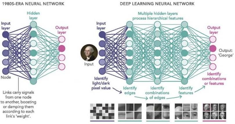
MobileNet Algorithm
 Deep Learning Transfer Learning

 Deep learning (DL) is a kind of machine learning based on ANN This algorithm runs almost like a classical CNN (Convolutive
 The principle of transfer learning is to use an already trained and

 [1]. It mimics the structure and process of the human brain as it Neuronal Network, several filtering and classifications of
 proven algorithm and modify the last layers to allow it to perform

 will decompose the tasks into various features performed one pictures). Only the convolution step is different. Indeed, for a
 a different but similar task. In our case, we will try to detect

 after an other. It can recognize representative data from CNN, the convolution is 3x3 size but, with MobileNet, the
 robots which were not part of the 90 classes present in the

 unstructured inputs (in contrast to Machine learning) and convolution is divided by 2 parts that we call depthwise
 provided MobileNet-V2 algorithm. The algorithm will be fine-tuned

 products specific actions or decisions. convolution and pointwise convolution.
 by retraining and should be able to detect a new class as it already

 Like machine learning, deep learning can be supervised or The depthwise convolution is 3x3 size and is used to
 acquired "skills" on the previous training.

 unsupervised. The main difference with a basic ANN is the number apply a single filter to each input channel (a channel of an image

 of layers of processing before the output (see FIG. 1). This allows represents a RGB level, so there are 3). Then, for the pointwise
 Jetson Nano 2GB specifications

 neural networks to automatically extract features from raw data convolution, this layer applies a convolution of 1x1 size to

 combine the outputs of depthwise convolution. Nvidia Jetson nano is a developer kit that has a builtin GPU
 without additional human input. Neural networks separate data
 In other terms, a standard convolution will take a picture with its composed of 128 cores, a CPU (Quad core) and 2 GB of RAM
 into chunks of data and send them to individual neurons of each
 channels and apply its filters then combine the results. (LPDDR4). It is designed to train DL computer vision algorithms
 layers for processing. Once each features have been completed,
 Conversely, MobileNet will apply filters to each channel and then in real time via USB webcam connection [6].
 the network produces the final output layer and makes a decision.
 will recombine the results (the depth of parallelepipeds on the There are other technologies that do the same but with different

 FIG.2 represents the channels) latency. This benchmark (in FIG.3) shows the time of latency (in

 fps) for a similar framework (Tensorflow) using different

 technologies (Jetson Nano, Raspberry, Intel Compute stick and

 Google edge TPU dev board).

 We can see that for our Model (ModelNet-v2), the jetson nano is

 faster than the Intel Neural Compute stick 2 but slower than the

 Google edge TPU dev board. However, there is a significant

 difference in price (150 euros for Google vs 70 euros for Jetson

 nano). Regarding the performance/ price ratio, Nvidia seems to
 FIG. 2: Depthwise convolution and Pointwise convolution
 be the best choice. Furthermore, Nvidia provides tutorials to learn

 and practice IA computer vision.

 MobileNet reduces computation times by a factor of 8 to 9

 compared to standard convolutions. However, the accuracy is also
 FIG. 1: Comparison between simple ANN and DL [3]
 reduced. In our case, it is more than enough to detect robots.

1 4 | RECHERCHE HEPL | 2022

 FIG. 3: Models performances on various boards
GPU over CPU METHODOLOGY AND TESTING
 Formatting data and creating directories

 We followed Nvidia tutorials [4] to understand how to adapt
 A CPU (central processing unit) works together with a GPU
 In order the use the training algorithm contained in the docker
 already existing algorithms and projects to create our own
 (graphics processing unit) to increase the throughput of data and
 container provided by Nvidia, various files and directories had to
 detection AI.
 the number of concurrent calculations within an application. GPUs
 be created. In the database directory,
 We firstly created a database of images containing robots. The
 were originally designed to create images for computer graphics
 3 other directories and a text file were created. We will explain
 database was then formatted to be compatible with the training
 and video game consoles, but since the early 2010’s, GPUs can
 their structure and their purpose.
 algorithm. Training was performed for around 30 epochs and the
 also be used to accelerate calculations involving massive amounts
 The "labels.txt" file must contain the name of the classes in
 created model was then exported into onnx. The detectnet
 of data.
 alphabetical order that we want the AI to detect.
 algorithm was then used to run the previously exported model
 A CPU can never be fully replaced by a GPU. A GPU complements
 In our case there is only one class : "robot". While training the
 and we were able to see the performances on real time camera
 CPU architecture by allowing repetitive calculations within an
 algorithm will automatically create a second class which is name
 feed. Finally, the database was updated and the model was
 application to be run in parallel while the main program continues
 "BACKGROUND" by default. In our case we want the algorithm to
 retrained
 to run on the CPU.
 only find robots and consider everything else on the image as
 and the results compared. A python program using detectnet
 The CPU can be thought of as the taskmaster of the entire system,
 background.
 and our model was written to display only the position of detected
 coordinating a wide range of general-purpose
 The "JPEGImages" directory will contain all our images in ".jpg"
 robots on the image.
 computing tasks, with the GPU performing a narrower range of
 format. Their size can be different but they should be renamed to
 more specialized tasks. Using the power of parallel-computing, a
 only contain basic characters and we renamed them "robotX" with
 Creation of the database
 GPU can perform more computation in the same amount of time
 X the number of the image for simplicity.
 as compared to a CPU.
 For the database we needed to find or take pictures of various The "Annotations" directory will contain a ".xml" file for each
 However, the presence of FPGAs in the electronic field allows to
 robots that are commonly used during robot contests (such as images. They are associated with the images using their names.
 compete with the GPUs by accelerating the neural networking
 Eurobot). We proceeded to find pictures of those kind of robot on They contain information about the bounding boxes that we
 process as FPGAs can also perform parallel-computing. In
 the internet (mainly using google image). created on each images to specify the position of the robots
 addition, FPGAs use lower power than GPU. Given that we have
 The objective was to find robots of different size and shapes in manually for training. In order to create those files we used a
 done a consumption study, this advantage would be beneficial to
 various situations. If we increase the number of pictures with program called "labelimg" provided by the user "tzutalin" on
 develop in the near future for better performance at low
 different camera angles and backgrounds, our model should be github [2].
 consumption.
 able to find robots in more situations than if we were to use only Finally the "ImageSets" directory contains another directory

 the same angle or the same background. In that case, changing called "Main" in which 4 text files can be found.

 the background would drastically reduce the performances of the Those files will list which images the algorithm should use for

 detection which is why we decided to provide those kind of training, validation and testing. A ratio of 80%/10%/10% is

 pictures. If we wanted to have a highly effective detection with recommended and has been used.

 the same point of view and the same background, we would have

 modified the database but in that kind of application the use of Training Algorithm

 deep learning might not be justified.
 For training the algorithm, the already provided by Nvidia
 The final database size was composed of 170 images.
 "train.py" file was used. The mobilenet algorithm was selected as
 Increasing the number of pictures and retrain the model should
 the base model for transfer learning and our training and
 increase the performances but would take a larger amount of
 validation sets were used to fine-tune mobilenet and obtain our
1 5 | RECHERCHE HEPL | 2022 training time.
 model.
We reduced the number of workers (limiting the parallel- Humans or other objects are sometimes mistaken for robots but

 computing power of the GPU) to avoid crashes and attain a robots are nearly always detected. Increasing the threshold value

 number of 30 epochs which is considered to be enough to get a for detection minimises the number of wrong objects detected but

 good detection. sometimes causes robots not to be detected.

 This limitation increased stability but increased the training time In order to improve the performances of the model, a larger robot

 (8 hours in total). After testing, the database was modified and database (over 1000 images in various backgrounds and point of

 the algorithm retrained. view) should be used. As such, several hours of training are

 FIG. 4: Power consumption with the Jetson Nano required because the number of images in the sets are larger and

 Exporting model and testing at least 30 epochs should be done. An important note for training

 is that too much epochs should be avoided as the over-fitting
 In order to export the model, the "onnx_export.py" file was used
 issue could arise (inducing the model to only be able to detect
 to convert our ".pth" file into an usable "onnx" model. The When comparing the MobileNets, we notice a slightly higher
 robots present in the database).
 detectnet program was then used to run our model and real-time consumption in MobileNetV1. Furthermore, MobileNetV1 is 4ms

 live video streaming was used to check the detection results. After faster than MobileNetV2. ResNet50 is the slowest, with a latency

 retraining the results were also compared and an improvement of 50ms. It is nearly 3 times slower than ResNet18. The power

 has been made. Finally, a custom detection Python file was consumption of the two ResNets are similar. ResNet18 consumes

 written a little bit more power than ResNet50. In general, MobileNets

 in order to retrieve only data regarding the position of detected are faster and more energy-efficient than ResNets at a

 robots with a set threshold (80% of certainty to display the comparable accuracy. The fastest inference and most energy-

 value). efficient classification can be achieved with MobileNetV1.

 When power is optimized, MobileNetV2 is 1% better than V1.

 Jetson Nano power consumption Smaller ResNets seem to be outdated; not only do they need
 FIG. 5: Robot detection with live camera
 much more power, but also, the latency is higher compared to
 We found a study[5] relative to the Jetson Nano power
 MobileNets.
 Power consumption
 consumption where a shunt resistor was placed in serial
 Our experiment with a shunt resistor allowed us to obtain those
 connection with the power supply and an oscilloscope was used
 plots FIG. 6 and FIG. 7µ
 to probe each end of the resistor. The current through the resistor RESULTS AND DISCUSSION
 is calculated using Ohm’s law. The product of this current with the

 input voltage results in power consumption. Detection

 In this study, the authors have selected four classification
 Detection of robots was achieved with our custom model as can
 networks : MobileNetV1, MobileNetV2, ResNet18, and ResNet50.
 be seen on FIG. 5. Moreover, the live camera feed detection can
 All of them were pre-trained for ImageNet classification. As an
 be observed and the position of the detected robots was
 input, they are used a tensor with a size of 3x224x224 like we
 extracted.
 did.
 The performances are good for a first approach with deep-learning

 detection algorithms but can still be greatly improved.

 FIG. 6: Power consumptions while running the Jetson Nano
1 6 | RECHERCHE HEPL | 2022
Using these plots, we have calculated the running mean value and ACKNOWLEDGMENTS
 the training mean value that are 5,18 W for the running mean

 value and 3.4716 W for the training mean value. It is important We would like to thank Professors Christophe BROSE, Sylvain

 to no tice that the training value can change and sometimes go GUICHAUX and Gilles SCHEEN for their continuous support and

 to 6W. The algorithm indicated a CPU latency of 32ms. advice during the realisation of this project. We are thankful for

 this opportunity, the resources and material they provided. We

 could not have achieved those results without them.

 [1] Deep Learning Goodfellow, Ian; Bengio, Yoshua; Courville,

 Aaron (2016)

 [2] https://github.com/tzutalin/labelImg

 [3] https://www.newworldai.com/what-is-deep-learningnature-

 of-machine-learning-and-beauty-of-deep-neuralnetwork

 [4] https://github.com/dusty-nv/jetson-inference

 [5] Profiling Energy Consumption of Deep Neural Networks

 on NVIDIA Jetson Nano. Stephan Holly, Alexander
 FIG. 7: Power consumptions while training the Jetson Nano
 Wendt, Martin Lechner

 [6] https://developer.nvidia.com/embedded/jetson-

 CONCLUSIONS nanodeveloper- kit

 [7] https://www.intel.fr/content/www/fr/fr/products/docs
 We have used the Jetson Nano AI kit developed by Nvidia and we
 /processors/movidius-vpu/myriad-x-product-brief.html
 have followed their tutorial to run an algorithm of objects
 [8] Fpgas and embedded vision applications. Vision systems
 detection. Then, we have learned to create our own database of
 design
 robot images to fine-tune a DL algorithm called MobileNet. After
 [9] Fpga vs gpu vs cpu hardware options for ai applications.
 training, we exported the model and achieved robot detection. We
 Avnet
 performed a power consumption study while the Jetson Nano
 [10] Cpu vs gpu. Omnisci
 training the model and when it was running it. Due to its high
 [11] https://www.le-coin-du-digital.com/index.php/2018/07/11/
 power consumption it may not be the best solution to interface
 deep-learning-vs-machine-learning Julie Lorenzini
 with a competition robot. Finally, we wrote a Python program that
 [12] Focus : MobileNet, une reconnaissance d’images temps
 sends directions when a robot is detected to avoid collision.
 réel et embarquée surpuissante. Lambert R.

 [13] Accelerating DNNs with Xilinx Alveo Accelerator Cards. Xilinx

1 7 | RECHERCHE HEPL | 2022
DESIGN OF A HIGH DATA-RATE
 WIRELESS COMMUNICATION ON
 FPGA - PART ONE

 G. Martin,1
 1
 Haute École de la Province de Liège
 (HEPL), electronic and embedded
 systems, Liège, Belgium
 January 2022

 This paper discusses about a high data-rate
 wireless communication implemented using a
 FPGA. The technologies chosen are QAM and 2.1.1 Spectral efficiency

 OFDM. A first version with low data-rate has been
 developed on a Zybo Z7 FPGA board using a digital The spectral efficiency of a given digital

 carrier architecture. Future versions of the project modulation scheme gives the data-rate

 will use more performant equipment and other TECHNOLOGY SELECTION achieved by one Hertz of the modulated signal’s

 architectures to increase both the carrier bandwidth. This is a critical aspect for

 frequency and the data rate. 2.1. Modulation techniques most of wireless communications systems.

 As reference, Bluetooth has a data-rate of about Table 1 shows the spectral efficiency (in
 INTRODUCTION 1M b/s and Wi-Fi 802.11a reaches 54M b/s.[1] Digital modulation techniques transfer data bits/s/Hz) of several modulation techniques.

 Frequency-division multiplexing will also be by changing the carrier signal properties : Quadrature Amplitude Modulation (QAM) allows
 Nowadays, the amount of data generated and
 discussed. frequency, amplitude and phase. The associated high-order modulation with several hundreds of
 consumed by digital devices increases constantly.
 This project will use FPGA technology because of techniques are called respectively symbols and has a better
 Wireless communications must be more and more
 its capability to compute processes quickly and the Frequency-Shift Keying (FSK), Amplitude- spectral efficiency than PSK. Increasing
 efficient and data-rate is a critical aspect. In this
 fact that it can deal with several processes in Shift Keying (ASK) and Phase-Shift Keying the amount of symbols does not wider the
 paper, we will compare several digital modulation
 parallel. (PSK) [2]. A more complex one called bandwidth of the modulated signal, which
 techniques and choose the one that matches the
 Quadrature Amplitude Modulation (QAM) means it increases spectral efficiency. The
 most our application : a 1Gb/s wireless
 applies variation to both amplitude and problem is that it will lead into a greater
 communication implemented using Field
 phase. It allows very high-order modulation Bit Error Rate (BER) because the demodulator
 Programmable Gate Arrays (FPGA).
 schemes. Modulation order being the uses euclidean distance between the
 amount of different carrier states used. I-Q point measured and the theoretical
1 8 | RECHERCHE HEPL | 2022
 constellation. | 9
2.2 Frequency-division multiplexing techniques
 Adding more symbols means less distance between the The fact of using several channels allows the communication to
 In order to increase the data-rate, one can increase the amount
 constellation’s points which leads to greater chances to mistake a be faster because data is sent through various carriers.
 of symbols in the modulation’s constellation. The problem is that
 symbol for another. The bit-rate is directly proportional to the amount of channels
 this approach has its limits because of the symbols discrimination.
 used.
 Another way is to spread the data flow on several channels,

 each one using a carrier at a different frequency. Simulations and developments
 This technique is called Frequency Division Multiplexing (FDM). It

 also allows to share the spectrum between users and peripherals. There are two carrier generation techniques : digital or analogical.

 The first one uses a Direct Digital Synthesiser (DDS) and all

 signals are digital until the end of the modulation.
 There are several FDM techniques but the most suitable one is
 The second technique uses a carrier generated by a local
 called Orthogonal Frequency-Division Multiplexing (OFDM).
 oscillator. Mixers are used to apply the I and Q components from
 2.1.2 Bit error rate This technology sends data through orthogonal channels, which
 the constellation. The two techniques are showed on figure 2.
 are separated by the minimum frequency theoretically achievable.

 The BER measures the amount of errors in the communication The spectrum value of one channel is zero at regular intervals and

 and needs to be minimized. the OFDM uses this property by spacing two consecutive

 In digital modulation, the technique that offers the best BER is channels by the value of that interval.

 FSK, followed by QAM then PSK and the worst is ASK [3]. It means that the centre of a channel is placed precisely at a

 Furthermore, an error of one symbol using QAM-4 or QAM-256 frequency where all other channels cancel [4]. This principle is

 means an error of respectively 2 bits and 8 bits. The more illustrated by the figure 1.

 symbols in the constellation, the more bits fail. This is why it is

 more efficient to have an adaptive system that changes the

 modulation order according to the BER. The BER depends on both
 3.1 Mapper
 the modulation technique and the modulation order.

 The mapper block in the figure 2 is composed of several Lookup
 2.1.3 Modulation choice
 Tables (LUTs) and is used to output I and Q values for a given

 symbol. It contains two LUTs (one for I and one for Q) for every
 The modulation that will be used for this project is the QAM
 modulation order.
 because of its spectral efficiency. FSK has better BER

 characteristics but is way worse as far as spectral efficiency This technique is the most efficient one but is also very difficult
 The values in those lookup tables represent the constellation
 is concerned [3]. to implement. This is why we will be using an easier method
 diagrams of every modulation scheme that will be used by the
 to start the project. This method also uses several channels but
 system. This means that all the carrier states (phase and
 the frequency interval between those is greater so they do not
 amplitude of the modulated carrier because QAM is used) are
 interfere with each others.
 defined inside the mapper.

1 9 | RECHERCHE HEPL | 2022
3.2.2 Sine wave generated
 3.2 Direct Digital Synthesiser

 The figure 4 shows the oscilloscope result of an approximatively
 For the first technique development (bottom in figure 2), a DDS
 1MHz sine wave generated using the DDS technique explained
 has been implemented in the FPGA using a sine wave LUT. The
 above.
 frequency of the output signal created can be configured using

 two methods : clock prescaling factor and the «frequency
 3.3.1 QAM-4 signals
 multiplier». The first reduces the clock frequency so each signal’s

 sample is output for a longer time. The second jumps over several
 The figure 5 shows the transition between two symbols on the
 LUT values, by skipping samples, the signal frequency
 modulated signal. The cursors are spaced by 256ns which is the
 increases.
 quarter of the carrier’s period (carrier frequency is 976.5625kHz
 Figure 3 shows the block diagram of the sine wave DDS.
 as seen in subsection 3.2.2). Therefore, it corresponds to a 90

 deg phase. As the two carrier states cross the x-axis on both the

 cursors, it means that the signal is shifted in phase by 90 deg.

 The modulation scheme used for this example is QAM-4 so the
 Figure 4: DDS generated sine wave amplitude between all the carrier states does not change.

 The sine wave values contained in the LUT have been computed
 The measured frequency is 976.6kHz and the theoretical
 using Matlab.
 frequency obtained with equation 1 is
 Using a Phase-Locked Loop (PLL) to feed the clock input could be
 125000000 .4
 = = 976,5625 which means that at this range of
 256 .2
 a great improvement in order to generate a sine wave at a specific
 frequency the sine wave generation is accurate.
 frequency. The limitations of the DDS block are still to be

 determined.
 3.3 Results on FPGA

 3.2.1 Theoretical generated frequency
 A first version of QAM-4 with a 1MHz DDS generated carrier have
 The LUT used contains 256 samples which means that with a
 been developed and tested on a Zybo Z7 FPGA board.
 frequency multiplier and a prescaling factor of one, the generated
 The symbol period is 100kHz which means the data-rate of this
 signal will last for 256 periods of the clock signal.
 first test is 200kb/s (100.000 2-bits symbols per second).
 Figure 5: Transition between two carrier states
 The equation 1 can be obtained using the same logic (with f out
 The resources used are summarized in the table 2. It shows that
 the frequency of the generated sine wave).
 this first version uses only a tiny portion of what is available 3.3.2 Data-rate measurement

 on the chip. Another important thing to notice is that this project The figure 6 shows the symbol period between the two cursors.

 will later be using another FPGA with more resources (for Each symbol has a duration of 10.18μs which means the

 example, it will have eight times more LUTs). modulated signal contains approximatively one hundred thousand

 of symbols per second.

 As the modulation used in this test is QAM- 4, each symbol
2 0 | RECHERCHE HEPL | 2022
 contains two bits of data, which leads to a 200kb/s data-rate.
CONCLUSIONS

 This paper described a work in progress.

 The major achievements here are the determination of the

 techniques that will be used in the future versions of the project

 and the discovering of the digital signal processing

 world using FPGA. The future improvements to do are : increase

 the carrier frequency, pulse shaping implementation, adaptive

 modulation order as well as everything concerning the

 demodulator.
 Figure 6: Symbol period of modulated signal
 Implementing the mixed architecture from figure 2 may be useful

 3.4 Spectrum simulation in order to compare with the already developed solution. Its

 analog components may simplify a lot the VHDL code for the
 As the carrier is still at a low frequency compared to what it should FPGA. The problem is that the mixers for I and Q must have the
 be in the future versions of the project, the modulated signal’s exact same characteristics or the modulation will not be a
 spectrum has not been measured yet on the output of the FPGA. success.
 A simulation using Simulink and Matlab has been made using the

 same system architecture as the one developed on the Zybo CONCLUSIONS
 Z7 board but with a 2.4GHz carrier and a symbol frequency of

 1MHz. The spectrum obtained is showed on the figure 7. It has
 [1] E. Ferro and F. Potorti, “Bluetooth and wi-fi wireless protocols:
 a maximum value at the carrier frequency and several local
 a survey and a comparison,” IEEE Wireless Communications, vol.
 minima separated by the symbol frequency .
 12, no. 1, pp. 12–26, 2005.

 [2] M. Barnela and D. S. Kumar, “Digital modulation schemes

 employed in wireless communication: A literature review,”

 International Journal of Wired and Wireless Communications,

 vol. 2, no. 2, pp. 15–21, 2014.

 [3] d. D. Françcois and R. Olivier, Electronique Appliquée aux

 Hautes Fréquences: Principes et Applications. Paris: Dunod, 2008.

 [4] Y. Wu and W. Zou, “Orthogonal frequency division

 multiplexing: a multi-carrier modulation scheme,” IEEE

 Transactions on Consumer Electronics, vol. 41, no. 3, pp. 392–

 Figure 7: Simulated spectrum of the modulated signal 399, 1995.

 [5] M. Rice, Digital communications: a discrete-time approach.

 Prentice Hall, 2009.

2 1 | RECHERCHE HEPL | 2022
TEST-PROTOTYPE DESIGN OF AN
 ISOLATED BIDIRECTIONNAL DC-
 DC CONVERTER FOR UPS
 APPLICATION

 Christophe Dejardin

 Haute Ecole de la Province de Liège
 January 2022

 This publication proposes the hardware design for

 a test-prototype of a bidirectional isolated dc-dc

 converter based on a dual full bridge with active CIRCUIT DESCRIPTION
 clamp converter model in order to create a UPS

 function for a micro-cogeneration boiler. Control The considered converter on fig. 2 has full bridges

 and measurement circuitry choices are proposed on each side of one isolation transformer to allow

 to optimally operate so that it can connect a 48V a large power transfer. The use of switches allows

 battery pack to a 380V bus and perform a two- the bridges to be in a role of inverter or

 way power transfer synchronous rectifier. Depending on the operating
 mosfets. On top of that, the possibility to have a
 direction, the converter will work in current-fed
 INTRODUCTION battery voltage variation over a wide range. Texas
 full bridge (boost mode) or voltage-fed full bridge
 Instrument published in 2016 a design reference
 (buck mode).
 To perform a bidirectional dc-dc conversion,
 of this type of converter. This does not exceed the
 several topologies are proposed in [1] and an ideal
 stage of proof-of-concept. We rely on the
 The topology of the dual full bridge converter is
 way to proceed is to design a single conversion
 operating modes they describe.
 equipped with a clamp branch to contain the
 stage. For our application shown in fig. 1, [2] lists
 However, the proposed circuits are not pragmatic
 numerous transients and to recover the leakage
 a few advantages that the full bridge with active
 and many circuits are not essential. This is why
 energy. Furthermore, as described in [3], it is
 clamp topology allows us to benefit from : reduced
 some relevant references will be proposed here.
 used to perform soft-switching, reducing the
 input-ripple current, optimization of the isolation
 They will be selected for an operating frequency of
 energy losses in high frequency operation.
 transformer, inherent protection against flux-
 100kHz.
 walking in the isolation transformer and the soft

 switching operated for the different pair of

 | 9
2 2 | RECHERCHE HEPL | 2022
In addition, in boost mode, the clamp branch allows to maintain the
 SWITCHING MOSFETS But in order to have a more known microcontroller, which has a

 voltage overshoot problem which appears at the closing of the bus- preferable development environment (STM32 Cube IDE) and
 For the battery side, the results obtained in [2] announce a peak
 side mosfets and to achieve a zero-voltage switching condition for reduced cost, the use of a STM32G4 microcontroller is proposed. The
 voltage at turnoff on the lowvoltage mosfet of 75V. The channel-n
 the current-fed side switches. [4] details the PWM control scheme of table 1 shows that the STM32 model has slightly better
 mosfet that will be used for the bridge and the clamp branch is a
 the mosfets to be in these conditions. characteristics than the one from Texas Instrument. The two
 SUP700E from Vishay, which supports a breakdown voltage of 100V.
 microcontrollers are provided on the board and the choice is made
 It has a low RDSON. This parameter is important to have ZVS
 In buck mode, it is a phase-shifted PWM signal type that allows to by soldering zero ohm resistors to activate the different control
 condition when turning off. It also has a low QG and QGD (142 nC
 achieve a zero-voltage zerocurrent condition for the bus-side signals
 and 18,5 nC) wich will condition the switching speed. The maximum
 switches and to reduce the losses. The converter also has a flyback
 needed current can be calculated (eq. 1) when charging the parasitic
 circuit connected to the main inductor to provide a "cold-start"
 capacitor. For a target rise time of 13 ns :
 mode, when the HV DC bus is completely discharged at start-up, and

 this to avoid voltage spike caused by the current difference between

 the current fed inductor and leakage inductance of the isolation

 transformer. It can also reduce the current flowing through the
 For the bus side, the model must be able to withstand a rapid high
 active switches.It works in this mode until the HV bus reaches 270-
 voltage change. The chosen channel-n mosfet is the IPA60R385CP
 V DC and then the system switches over, to work as a current-fed
 from Infineon. Its breakdown voltage goes up to 650V and it
 converter.
 supports dv/dt values of 15V/ns.

 CONTROL AND DRIVING
 Gate drivers
 For the low voltage side gate drivers, two isolated half bridge gate

 drivers (Adum4223) from Analog Device are selected. Insulation is

 not mandatory but it ensures a good EMC. They can deliver a

 source current of 4A (enough for the SUP70030E). They work up to

 a frequency of 8 Mhz and have a disable function. The power

 BATTERY supply of the upper MOSFET driver is done by a bootstrap circuit

 which has the advantage of an external bootstrap diode which does
 The battery type proposed for this set-up is LiFePo4. Compared to
 not directly heat the driver. For the high voltage side gate drivers,
 other types of lithium accumulators [5], they have lower capacitance
 two half bridge gate drivers (Si8233) from Skyworks are now
 and lower power density. However, as mentionned in [6], this type
 proposed. They allow an isolated control required for the 380V
 has safety overriding criterion for use as a UPS system and in the Control
 side. They also have a deadtime function to define a delay between
 co-generation boiler working environment. Indeed, this battery has Fig. 3 shows the different control circuits. For testing purposes, two
 the switching of the two mosfets of the branch to avoid a short
 non-toxic material and is not overheated or catches fire in case of different MCUs are deployed. The first is the DSP TMS320F2803
 circuit which would be extremely damaging.
 overcharging or overload. This type also has features such as lower proposed by Texas Instrument. At first, the use of this one is
 The drivers of the clamping and flyback circuits are AduM3123 1-
 cost, and longer cycle life. envisaged, because its operation has already been demonstrated.
 channel from Analog Device. They allow an isolated control and

 have a disable function. All deactivation signals will be linked into
2 3 | RECHERCHE HEPL | 2022
 one and it will be activated when a security state is active.
MEASUREMENTS Temperature measurement
 Fig.6 shows the power stage organization. The clamp and flyback
 For the temperature measurement, we could provide NTCs to be
 drivers control side are referenced on the LV side. For the bus side
 screwed on each radiators. This allows a precise measurement as
 gate driver, an isolated 12V supply is set up to avoid external noises.
 close as possible to the radiators. The measurements will also be
 The R12P12S dc/dc module from RECOM provides 6.4 kVDC isolation
 sent to the OPA48.
 and up to 2W power.

 PCB DESIGN

 The measurement of different currents, voltages and temperatures

 is necessary for regulation, intelligent monitoring, safety and load

 balancing. Fig. 4 shows where these measurement elements are

 positioned.

 Current measurement

 Two current measurements are necessary. One at the upper level of

 the bridge on the battery side and one at the transformer secondary

 side. CKSR Current transducers from LEM are proposed. They allow COMMUNICATION
 the isolated and bidirectional measurement of the converter
 Two communications are provided: one to the battery management
 currents. They also allow the measurement of
 system and one to a higher control board. These are done with the
 pulsed current (IBUS). The transducer provides a differential
 RS485 communication protocol. It is a protocol that counts some
 measurement that we scale and convert into an single-ended signal
 criteria necessary to operate in a harsh environment. Especially, a
 to connect directly to the microcontroller. For the low side, where
 differential communication that provides good noise immunity, and
 the current will be the highest, the peak current can reach 47 A (for
 also faster communication, low level interface. An additional
 a 2280W battery). The CKSR-50 is recommended while for the high
 insulation can be thought between the mcu and the outside of the
 side, the CKSR-15 is sufficient (5A peak at 380VDC).
 system as illustrated in fig.5. For this purpose, two ISOW1485

 modules are used. They allow an isolated communication
 Voltage measurement

 Three measurements are proposed: The voltage on the battery side,
 POWER STAGE
 the voltage on the bus side and the auxiliary 12V voltage from which

 the other voltage levels are also generated.
 Fig. 7 shows the top view of the pdb and fig. 8 shows the 3D
 For the bus voltage, a measurement of the voltage divider by an
 representation in Altium designer. In terms of layout, the low level
 isolated amplifier of high precision is used. It is the AMC3330 from
 and high level parts are separated by good isolation distances. To
 Texas Instrument. It has the advantage of having an integrated
 save space, the circuitry of the texas mcu is positioned under the
 isolated DC-DC converter to supply the isolated part.
 nucleo board, between its terminal blocks. The design is made in two
 For the voltage on the battery side and auxiliary 12V, an OPA48 is
 layers.
 sufficient

2 4 | RECHERCHE HEPL | 2022

 .
CONCLUSION REFERENCES

 [1] A Geetha, N.P. Subramanian, R. Gnanadass, “Operation if
 In this paper, a brief description of the circuit is done and new
 current-fed Dual Active Bridge DCDC Converters for Microgrid,” in
 references are proposed for the main modules needed to operate the
 International Journal of Recent Technology and Engineering (IJRTE),
 converter, while paying attention to the important parameters. A
 2019, pp. 3167-3175.
 next step is to proceed to new tests with the proposed circuits and
 [2] Sivakumar R, “Designing a high-efficiency, isolated bidirectionnal
 thus obtain values to characterize output ripple, transition time,
 power converter for a UPS,” in Analog application Journal, 2017.
 startup, switching stress and so on. This publication can help
 [3] Jung G.Cho, Geun H. Rim, « Zero Voltage and Zero Current
 potential circuit designers to deploy this type of converter for the
 Switching Full Bridge PWM Converter Using Secondary Active Clamp,
 studied value range.
 » 1996, in IEEE, pp 657-663.

 [4] Kunrong Wang, V., F. C. Lee, and Jason Lai, “ operation principles

 of bi-directional full-bridge dcdc converter with unified soft-switching

 scheme and softstarting capability ” , 2000, pp. 111-118.

 [5] G. Albright, J Edie and S aL-Hallaj, « A Comparison of Lead Acid

 to Lithium-ion in Stationary Storage Applications », AllCell

 Technologies LLC, 2012.

 [6] BA Anandh, A Shankar Ganesh, R Sakthivel, D Mahesh Kumar, E

 Prem Kumar, «Smart Battery Management System Using LiFePO4

 Battery for Offline UPS » , in al 2021 J. Phys.: Conf. Ser

2 5 | RECHERCHE HEPL | 2022
ème
 Les étudiantsWant toingénieurs desmell2like
 make the bathroom a
 Bachelier onttropical
 été vacation?
 confrontés pour la
 première fois à la littérature scientifique!
 Perhaps your office needs to be uplifted
 with the smell of freshly brewed coffee?

 Au cours « Scientific Littérature », les
 étudiants ont dû rédiger un article de
 synthèse se basant sur l’état de l’art
 dans une thématique relevant de la
 Sciences des matériaux.

 Un travail ardu , parfois maladroit mais
 qui met en lumière la curiosité et
 l’enthousiasme de nos étudiants.

2 6 | RECHERCHE HEPL | 2022
MINI-REVUE : ANALYSE DES MÉTHODES DE LA
 FABRICATION ADDITIVE ET IDENTIFICATION
 DES DÉFAUTS LORS DE LA FABRICATION DES
 MÉTAUX.

 Laurien Colinet, Delforge Alexandra, Hoppe Simon, Madani Ziad, Sevello Alice, Demy
 Philippe
 Haute Ecole de la Province de Liège, Département Sciences et Techniques.

 Janvier 2022

 L’Additive Manufacturing est une technique de

 fabrication utilisant notamment des lasers

 sélectifs et de fusion par faisceaux d’électrons. Ces technologie soit encore assez récente, il existe
 méthodes permettent de fabriquer des pièces Ceux-ci peuvent entraîner des effets plusieurs méthodes de fabrication additive,
 complexes dans le domaine de l’industrie de catastrophiques sur les propriétés mécaniques des comme le SL (Laser sélectif) ou encore le EBM.
 l’aérospatial ou de la biotechnologie. Les pièces. Il faut donc trouver un moyen de Mais peu importe la méthode, certains défauts lors
 différentes méthodes utilisent toutes un lit de minimiser voire éliminer ces défauts. Les INTRODUCTION de la création de la pièce apparaissent en nombres
 poudre. Ce lit de poudre est ajouté couche par techniques utilisées sont diverses et non négligeables et ils doivent être éliminés.
 couche et les particules le constituant sont majoritairement appliquées après la construction L’« additive manufacturing », aussi connue sous
 Cet article a pour but de faire le point sur les
 fusionnées. Le laser et le faisceau d’électrons sont de la pièce. Il s’agit soit de méthode mécanique le nom AM est un processus permettant de
 différences entre trois techniques différentes
 utilisés pour faire fondre les poudres et ainsi comme le sablage, soit chimique comme la produire des pièces nettes à partir de différents
 d’AM, essentiellement dans les matériaux
 obtenir une pièce métallique. Malgré que l’Additive gravure chimique. Il existe également des moyens types de matériaux. Ces matériaux peuvent être
 métalliques. Ensuite, les cause d’apparition des
 Manufacturing offre un bon nombre d’avantages, pour minimiser l’apparition des défauts lors de la des polymères, des céramiques ou encore des
 défauts lors de la fabrication des pièces en
 la technique présente pas mal de défauts, tels que création de la pièce, comme chauffer le lit de métaux [1]. Cette méthode de fabrication additive
 fonction de la méthode utilisée seront évoquées.
 la contrainte résiduelle et les porosités. Certains poudre pour diminuer le gradient de température, est utilisée en industrie pour construire des pièces
 Enfin, l’article se terminera par une synthèse des
 défauts sont propres à la méthode utilisée comme mais ces moyens ne sont malheureusement pas très complexes notamment dans le domaine de
 différentes méthodes connues pour minimiser la
 les fissures pour la méthode de fusion sélective les plus efficaces. l’aérospatial ou des prothèses [2]. Certaines
 présence et l’apparition des défauts.
 par Laser et les pertes de bords pour la fusion par pièces indispensables dans ces milieux sont

 faisceau d’électrons. pratiquement inconcevables manuellement ce qui

 donne une importance capitale à cette méthode de

 fabrication. Malgré le fait que cette

2 7 | RECHERCHE HEPL | 2022
Ensuite, la plateforme s’abaisse couche après couche jusqu’à ce que 2.2. Méthode EBM : Electron Beam Melting
 METHODE GENERALE : Powder Bed Fusion la pièce soit terminée.

 Les couches de poudre ont une épaisseur entre 50 et 200 µ [3]. C’est la fusion par faisceau d’électron. Cette méthode de fabrication

 La fusion sur lit de poudre (PBF) est un processus de fabrication Pour terminer, la pièce est laissée jusqu’à ce qu’elle soit refroidie additive utilise un faisceau d’électron de haute énergie afin de faire

 additive qui utilise soit un laser (SLS et SLM) ou soit un faisceau pour éviter toute déformation. Après cela, elle est nettoyée des fondre la poudre métallique. Cette technique a été notamment

 d’électrons (EBM) comme source d’énergie. Ces deux sources vont excès de poudre qui n’auraient pas fusionner durant le processus de développée en utilisant une autre méthode. Elle est appelée

 permettre de fusionner des particules de poudre métallique afin de fabrication. microscopie électronique à balayage (SEM). Cette dernière utilise un

 former une pièce. Voyons en détail ces deux types de méthodes. fin faisceau d’électrons émis par un canon à électrons et des lentilles

 2.1.2. Méthode SLM : Selective Laser Melting électromagnétiques permettant de focaliser le faisceau d’électrons

 2.1. Méthode SL sur l’échantillon [5].

 Il existe deux principales méthodes SL : le frittage sélectif par laser (SLS) C'est une méthode qui comporte plusieurs étapes. D'abord, le laser Pour l’EBM, on passe par plusieurs étapes. D’abord, on focalise le

 et la fusion sélective par laser (SLM). Ces deux méthodes permettent de à haute puissance va fusionner des fines particules de métal. Il va faisceau d’électrons par le système de lentilles électromagnétiques

 créer des pièces métalliques à l’aide d’un laser chauffant la poudre. La être guidé à partir d’un ordinateur, ce qui va donc permettre au laser puis, une trémie à poudre verse celle-ci sur le côté de la plate-forme

 différence réside dans la fusion des poudres. La méthode SLS ne fond pas de suivre un tracé bien déterminé. Ce dernier va donc faire et enfin une couche de poudre est enduite par un râteau sur le

 les molécules de poudres. Elle les chauffe pour que ces dernières fondre les particules de métal jusqu’à ce qu’elles ne forment qu’une dessus de la couche préalablement fondue (voir Figure 2).

 adhèrent entre elles (collage). Par contre, la méthode SLM fait fondre la seule et même particule, c’est-à-dire, qu’elles fusionnent entre-elles.

 poudre. Par la suite, une nouvelle couche de poudre va être déposée par une

 sorte de rouleau, comme indiqué à la Figure 1 et le laser va de
 2.1.1. Méthode SLS : Selective Laser Sintering
 nouveau former une couche. Cela va se reproduire plusieurs fois

 jusqu’à obtention de la pièce métallique souhaitée. Lorsque c’est
 Il s’agit d’un procédé de fabrication additive qui utilise un laser à terminé, il faut attendre que la pièce métallique soit refroidie pour
 haute puissance pour “fritter”. Autrement dit, il soumet des pièces pouvoir l’enlever du baquet de poudre. Cela évite d’éventuelles
 métalliques à un frittage pour créer une structure solide [3]. déformations de la pièce. Pour terminer, la pièce est nettoyée pour

 retirer tous les restes de particules de poudre qui n’auraient pas Figure 2 : Schématisation des composants de la méthode EBM [5].
 C'est une méthode divisée en plusieurs étapes. Pour commencer,
 fusionner [4].
 dans une chambre de fabrication, de la poudre est déposée sur une IDENTIFICATION DES DEFAUTS
 plateforme en fine couche. L'imprimante va préchauffer la poudre à
 Même si les méthodes de production sont différentes, elles ont un
 une température un peu inférieur au point de fusion de la matière
 point commun : les défauts de fabrication. Bien que chaque méthode
 première. Ainsi, le laser va pouvoir s’élever plus facilement à la
 n’engendre pas toujours les mêmes défauts lors de la fabrication que
 température des zones spécifiques au lit de poudre pour avoir la Figure 1 : Illustration schématique de la méthode SLM [4].
 les autres, il y en a certains qui sont récurrents comme l’apparition
 forme du modèle de la pièce recherchée. Le laser va chauffer la
 de porosités ou les contraintes résiduelles.
 poudre en balayant une section, dite transversale, de la forme de la
 Par exemple dans le cas d’un alliage de titane Ti-6Al-4V, il y a 3.1. Défauts généraux
 pièce. Par conséquent, cela va fusionner les particules de métal entre
 création d’une structure martensitique ce qui augmente nettement 3.1.1. Porosités
 elles pour obtenir la pièce métallique sous forme solide.
 la résistance à la fatigue [2]. Les porosités sont des défauts qui se retrouvent dans toutes les

 méthodes de fabrication des métaux par fabrication additive. Il

 s’agit d’un vide sphérique microscopique, aux alentours de 100µm

 (voir Figure 3), fermés sous la surface de la pièce.
2 8 | RECHERCHE HEPL | 2022
Vous pouvez aussi lire