DÉMARRER AVEC KICAD - KICAD DOCS
←
→
Transcription du contenu de la page
Si votre navigateur ne rend pas la page correctement, lisez s'il vous plaît le contenu de la page ci-dessous
Démarrer avec KiCad
Démarrer avec KiCad                   ii

                      22 avril 2019
Démarrer avec KiCad iii
Table des matières
1 Introduction à KiCad 1
1.1 Downloading and installing KiCad . . . . . . . . . . . . . . . . . . . . . . . . . . . . . . . . . . . . . . . . . . 1
1.1.1 Sous GNU/Linux . . . . . . . . . . . . . . . . . . . . . . . . . . . . . . . . . . . . . . . . . . . . . . . 2
1.1.2 Under Apple macOS . . . . . . . . . . . . . . . . . . . . . . . . . . . . . . . . . . . . . . . . . . . . . 2
1.1.3 Sous Windows . . . . . . . . . . . . . . . . . . . . . . . . . . . . . . . . . . . . . . . . . . . . . . . . 2
1.2 Assistance . . . . . . . . . . . . . . . . . . . . . . . . . . . . . . . . . . . . . . . . . . . . . . . . . . . . . . . 3
2 Echanges de données dans KiCad 4
2.1 Overview . . . . . . . . . . . . . . . . . . . . . . . . . . . . . . . . . . . . . . . . . . . . . . . . . . . . . . . 4
2.2 Annotations et rétro-annotations . . . . . . . . . . . . . . . . . . . . . . . . . . . . . . . . . . . . . . . . . . . 6
3 Using KiCad 7
3.1 Shortcut keys . . . . . . . . . . . . . . . . . . . . . . . . . . . . . . . . . . . . . . . . . . . . . . . . . . . . . 7
3.1.1 Accelerator keys . . . . . . . . . . . . . . . . . . . . . . . . . . . . . . . . . . . . . . . . . . . . . . . 7
3.1.2 Hotkeys . . . . . . . . . . . . . . . . . . . . . . . . . . . . . . . . . . . . . . . . . . . . . . . . . . . . 7
3.1.3 Example . . . . . . . . . . . . . . . . . . . . . . . . . . . . . . . . . . . . . . . . . . . . . . . . . . . 8
4 Dessiner des schémas électroniques 9
4.1 Utiliser Eeschema . . . . . . . . . . . . . . . . . . . . . . . . . . . . . . . . . . . . . . . . . . . . . . . . . . . 9
4.2 Connexions par bus avec KiCad . . . . . . . . . . . . . . . . . . . . . . . . . . . . . . . . . . . . . . . . . . . 19
5 Router le circuit imprimé (PCB) 21
5.1 Utiliser Pcbnew . . . . . . . . . . . . . . . . . . . . . . . . . . . . . . . . . . . . . . . . . . . . . . . . . . . . 21
5.2 Générer les fichiers Gerber . . . . . . . . . . . . . . . . . . . . . . . . . . . . . . . . . . . . . . . . . . . . . . 28
5.3 Utiliser GerbView . . . . . . . . . . . . . . . . . . . . . . . . . . . . . . . . . . . . . . . . . . . . . . . . . . . 29
5.4 Routage automatique avec FreeRouter . . . . . . . . . . . . . . . . . . . . . . . . . . . . . . . . . . . . . . . . 29
6 Les Annotations dans KiCad 30
7 Make schematic symbols in KiCad 31
7.1 Utiliser l’Editeur des Librairies Schématiques . . . . . . . . . . . . . . . . . . . . . . . . . . . . . . . . . . . . 31
7.2 Exporter, Importer et modifier une librairie . . . . . . . . . . . . . . . . . . . . . . . . . . . . . . . . . . . . . . 33
7.3 Créer un symbole de composant avec QuickLib . . . . . . . . . . . . . . . . . . . . . . . . . . . . . . . . . . . 34
7.4 Créer un symbole de composant avec un grand nombre de broches . . . . . . . . . . . . . . . . . . . . . . . . . 34Démarrer avec KiCad iv
8 Créer une empreinte de composant 37
8.1 Utiliser l’Editeur d’Empreintes . . . . . . . . . . . . . . . . . . . . . . . . . . . . . . . . . . . . . . . . . . . . 37
9 Portabilité des fichiers d’un projet KiCad 39
10 Documentation complémentaire à propos de KiCad 40
10.1 La documentation de KiCad sur l’internet . . . . . . . . . . . . . . . . . . . . . . . . . . . . . . . . . . . . . . 40Démarrer avec KiCad v Prise en main rapide des principales fonctionnalités de KiCad pour la conception de circuits imprimés électroniques sophisti- qués. Copyright This document is Copyright © 2010-2018 by its contributors as listed below. You may distribute it and/or modify it under the terms of either the GNU General Public License (http://www.gnu.org/licenses/gpl.html), version 3 or later, or the Creative Commons Attribution License (http://creativecommons.org/licenses/by/3.0/), version 3.0 or later. Toutes les marques apparaissant dans ce document appartiennent à leurs propriétaires respectifs. Contributeurs David Jahshan, Phil Hutchinson, Fabrizio Tappero, Christina Jarron, Melroy van den Berg, Marc Berlioux. Traduction Pierre Beneteau , 2015. Martin d’Allens , 2015. Marc Berlioux , 2015-2016. Retours Merci de signaler vos corrections de bugs, suggestions ou nouvelles versions ici : — Documentation de KiCad : https://github.com/KiCad/kicad-doc/issues — Bugs logiciel KiCad : https://bugs.launchpad.net/kicad — About KiCad software internationalization (i18n): https://github.com/KiCad/kicad-i18n/issues Date de publication 16 mai 2015.
Démarrer avec KiCad                                                                                                           1 / 40

Chapitre 1

Introduction à KiCad

KiCad est un logiciel open-source destiné à la création de schémas électroniques et de circuits imprimés. D’apparence monoli-
thique, KiCad est en réalité composé de plusieurs logiciels spécifiques qui coopèrent :

  Program name                                Description                                File extension
  KiCad                                       Project manager                            *.pro
  Eeschema                                    Schematic and component editor             *.sch, *.lib, *.net
  Pcbnew                                      Circuit board and footprint editor         *.kicad_pcb, *.kicad_mod
  GerbView                                    Gerber and drill file viewer               *.g\*, *.drl, etc.
  Bitmap2Component                            Convert bitmap images to components        *.lib, *.kicad_mod, *.
                                              or footprints                              kicad_wks
  PCB Calculator                              Calculator for components, track           None
                                              width, electrical spacing, color codes,
                                              and more. . .
  Pl Editor                                   Page layout editor                         *.kicad_wks

  Note
  The file extension list is not complete and only contains a subset of the files that KiCad supports. It is useful for the basic
  understanding of which files are used for each KiCad application.

KiCad peut être considéré comme suffisamment abouti pour servir à la conception et la maintenance de cartes électroniques
complexes.
KiCad n’a aucune limitation de taille des circuits imprimés et peut facilement gérer jusqu’à 32 couches de cuivre, jusqu’à 14
couches techniques, et 4 couches auxiliaires. KiCad peut créer tous les fichiers nécessaires à la génération de cartes électroniques
et notamment des fichiers Gerber pour photo-traceurs, des fichiers de perçage, des fichiers d’implantation des composants etc.
Étant open-source (licence GPL), KiCad est l’outil idéal pour la création de matériel électronique orienté open-source ou open-
hardware.
On the Internet, the homepage of KiCad is:
http://www.kicad-pcb.org/

1.1    Downloading and installing KiCad

KiCad runs on GNU/Linux, Apple macOS and Windows. You can find the most up to date instructions and download links at:
http://www.kicad-pcb.org/download/
Démarrer avec KiCad 2 / 40
Important
KiCad stable releases occur periodically per the KiCad Stable Release Policy. New features are continually being
added to the development branch. If you would like to take advantage of these new features and help out by testing
them, please download the latest nightly build package for your platform. Nightly builds may introduce bugs such as file
corruption, generation of bad Gerbers, etc., but it is the goal of the KiCad Development Team to keep the development
branch as usable as possible during new feature development.
1.1.1 Sous GNU/Linux
Des versions stables de KiCad peuvent être trouvées dans la plupart des gestionnaires de distributions tels que kicad et kicad-doc.
Si votre distribution ne fournit pas la dernière version stable, suivez les instructions pour les versions instables
Sous Ubuntu, la façon la plus facile d’installer une version instable de KiCad est de passer par les dépôts PPA et Aptitude. Tapez
dans un terminal les commandes suivantes :
sudo add-apt-repository ppa:js-reynaud/ppa-kicad
sudo aptitude update && sudo aptitude safe-upgrade
sudo aptitude install kicad kicad-doc-en
Under Debian, the easiest way to install backports build of KiCad is:
# Set up Debian Backports
echo -e "
# stretch-backports
deb http://ftp.us.debian.org/debian/ stretch-backports main contrib non-free
deb-src http://ftp.us.debian.org/debian/ stretch-backports main contrib non-free
" | sudo tee -a /etc/apt/sources.list > /dev/null
# Run an Update & Install KiCad
sudo apt-get update
sudo apt-get install -t stretch-backports kicad
Sous Fedora, la façon la plus facile d’installer une version instable de KiCad est de passer par copr. Pour installer KiCad en
utilsant copr, tapez ce qui suit dans copr :
sudo dnf copr enable mangelajo/kicad
sudo dnf install kicad
Vous pouvez cependant télécharger et installer une version pré-compilée de KiCad ou bien télécharger le code source, le compiler
et installer KiCad.
1.1.2 Under Apple macOS
Stable builds of KiCad for macOS can be found at: http://downloads.kicad-pcb.org/osx/stable/
Des versions instables (compilées quotidiennement) pour OS X peuvent être trouvées à : http://downloads.kicad-pcb.org/osx/
1.1.3 Sous Windows
Des versions stables de KiCad pour Windows peuvent être trouvées à : http://downloads.kicad-pcb.org/archive/
Des versions instables (compilées quotidiennement) pour Windows peuvent être trouvées à : http://downloads.kicad-pcb.org/-
windows/Démarrer avec KiCad 3 / 40 1.2 Assistance Si vous avez des idées, des remarques, des questions ou si vous avez besoin d’aide : — Visit the forum — Rejoignez le Canal IRC #kicad sur Freenode — Watch tutorials
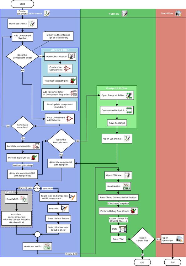
Démarrer avec KiCad                                                                                                      4 / 40

Chapitre 2

Echanges de données dans KiCad

Despite its similarities with other PCB design software, KiCad is characterised by a unique workflow in which schematic com-
ponents and footprints are separate. Only after creating a schematic are footprints assigned to the components.

2.1    Overview

The KiCad workflow is comprised of two main tasks: drawing the schematic and laying out the board. Both a schematic com-
ponent library and a PCB footprint library are necessary for these two tasks. KiCad includes many components and footprints,
and also has the tools to create new ones.
In the picture below, you see a flowchart representing the KiCad workflow. The flowchart explains which steps you need to take,
and in which order. When applicable, the icon is added for convenience.
Démarrer avec KiCad 5 / 40
Démarrer avec KiCad                                                                                                           6 / 40

For more information about creating a component, read Making schematic symbols. And for information about how to create a
new footprint, see Making component footprints.
Quicklib is a tool that allows you to quickly create KiCad library components with a web-based interface. For more information
about Quicklib, refer to Making Schematic Components With Quicklib.

2.2    Annotations et rétro-annotations

Once an electronic schematic has been fully drawn, the next step is to transfer it to a PCB. Often, additional components might
need to be added, parts changed to a different size, net renamed, etc. This can be done in two ways: Forward Annotation or
Backward Annotation.
Forward Annotation is the process of sending schematic information to a corresponding PCB layout. This is a fundamental
feature because you must do it at least once to initially import the schematic into the PCB. Afterwards, forward annotation allows
sending incremental schematic changes to the PCB. Details about Forward Annotation are discussed in the section Forward
Annotation.
Backward Annotation is the process of sending a PCB layout change back to its corresponding schematic. Two common causes
for Backward Annotation are gate swaps and pin swaps. In these situations, there are gates or pins which are functionally
equivalent, but it may only be during layout that there is a strong case for choosing the exact gate or pin. Once the choice is made
in the PCB, this change is then pushed back to the schematic.
Démarrer avec KiCad                                                                                                     7 / 40

Chapitre 3

Using KiCad

3.1     Shortcut keys

KiCad has two kinds of related but different shortcut keys: accelerator keys and hotkeys. Both are used to speed up working in
KiCad by using the keyboard instead of the mouse to change commands.

3.1.1   Accelerator keys

Accelerator keys have the same effect as clicking on a menu or toolbar icon: the command will be entered but nothing will
happen until the left mouse button is clicked. Use an accelerator key when you want to enter a command mode but do not want
any immediate action.
Accelerator keys are shown on the right side of all menu panes:

3.1.2   Hotkeys

A hotkey is equal to an accelerator key plus a left mouse click. Using a hotkey starts the command immediately at the current
cursor location. Use a hotkey to quickly change commands without interrupting your workflow.
To view hotkeys within any KiCad tool go to Help → List Hotkeys or press Ctrl+F1:
Démarrer avec KiCad                                                                                                              8 / 40

You can edit the assignment of hotkeys, and import or export them, from the Preferences → Hotkeys Options menu.

  Note
  In this document, hotkeys are expressed with brackets like this: [a]. If you see [a], just type the "a" key on the keyboard.

3.1.3   Example

Consider the simple example of adding a wire in a schematic.
To use an accelerator key, press "Shift + W" to invoke the "Add wire" command (note the cursor will change). Next, left click on
the desired wire start location to begin drawing the wire.
With a hotkey, simply press [w] and the wire will immediately start from the current cursor location.
Démarrer avec KiCad                                                                                                          9 / 40

Chapitre 4

Dessiner des schémas électroniques

Dans cette section, nous allons apprendre comment dessiner un schéma électronique avec KiCad.

4.1    Utiliser Eeschema

  1. Sous Windows exécutez kicad.exe. Sous Linux tapez kicad dans votre Terminal. Vous êtes maintenant dans la fenêtre
     principale du gestionnaire de projet de KiCad. A partir de cette fenêtre, vous avez accès à huit outils indépendants :
     Eeschema, Editeur de Librairies, Pcbnew, Editeur d’empreintes PCB, GerbView, Bitmap2Component, PCB Calculator et
     Pl Editor. Référez-vous au diagramme précédent pour un aperçu de la façon d’utiliser ces différents outils.

  2. Create a new project: File → New → Project. Name the project file tutorial1. The project file will automatically take the
     extension ".pro". The exact appearance of the dialog depends on the used platform, but there should be a checkbox for
     creating a new directory. Let it stay checked unless you already have a dedicated directory. All your project files will be
     saved there.

  3. Commençons par créer un schéma. Lancer l’éditeur de schémas Eeschema                   . C’est le premier bouton à gauche.

  4. Click on the Page Settings icon        on the top toolbar. Set the appropriate paper size (A4,8.5x11 etc.) and enter the Title
     as Tutorial1. You will see that more information can be entered here if necessary. Click OK. This information will populate
     the schematic sheet at the bottom right corner. Use the mouse wheel to zoom in. Save the whole schematic: File → Save

  5. We will now place our first component. Click on the Place symbol icon            in the right toolbar. You may also press the
     Add Symbol hotkey [a].
  6. Click on the middle of your schematic sheet. A Choose Symbol window will appear on the screen. We’re going to place a
     resistor. Search / filter on the R of Resistor. You may notice the Device heading above the Resistor. This Device heading is
     the name of the library where the component is located, which is quite a generic and useful library.
Démarrer avec KiCad 10 / 40
7. Double click on it. This will close the Choose Symbol window. Place the component in the schematic sheet by clicking
where you want it to be.
8. Cliquez sur l’icône de loupe pour zoomer sur le composant, ou utilisez la molette de la souris. Un clic sur la molette
(bouton central) permet de se déplacer horizontalement ou verticalement.
9. Try to hover the mouse over the component R and press [r]. The component should rotate. You do not need to actually
click on the component to rotate it.
Note
Sometimes, if your mouse is also over something else, a menu will appear. You will see the Clarify Selection menu often
in KiCad; it allows working on objects that are on top of each other. In this case, tell KiCad you want to perform the action
on the Symbol . . . R. . . if the menu appears.
10. Right click in the middle of the component and select Properties → Edit Value. You can achieve the same result by
hovering over the component and pressing [v]. Alternatively, [e] will take you to the more general Properties window.
Notice how the right-click menu below shows the hotkeys for all available actions.Démarrer avec KiCad 11 / 40
11. The Edit Value Field window will appear. Replace the current value R with 1 k. Click OK.
Note
Do not change the Reference field (R?), this will be done automatically later on. The value above the resistor should now
be 1 k.
12. To place another resistor, simply click where you want the resistor to appear. The symbol selection window will appear
again.
13. La résistance que vous avez choisi précédemment apparaît dorénavant dans la liste Historique. Cliquez sur R puis sur OK
et placez le composant.Démarrer avec KiCad 12 / 40
14. In case you make a mistake and want to delete a component, right click on the component and click Delete. This will
remove the component from the schematic. Alternatively, you can hover over the component you want to delete and press
[Delete].
15. You can also duplicate a component already on your schematic sheet by hovering over it and pressing [c]. Click where you
want to place the new duplicated component.
16. Right click on the second resistor. Select Drag. Reposition the component and left click to drop. The same functionality
can be achieved by hovering over the component and by pressing [g]. [r] will rotate the component while [x] and [y] will
flip it about its x- or y-axis.
Note
Right-Click → Move or [m] is also a valuable option for moving anything around, but it is better to use this only for
component labels and components yet to be connected. We will see later on why this is the case.
17. Edit the second resistor by hovering over it and pressing [v]. Replace R with 100. You can undo any of your editing actions
with Ctrl+Z.
18. Change the grid size. You have probably noticed that on the schematic sheet all components are snapped onto a large pitch
grid. You can easily change the size of the grid by Right-Click → Grid. In general, it is recommended to use a grid of
50.0 mils for the schematic sheet.
19. We are going to add a component from a library that may not be configured in the default project. In the menu, choose
Preferences → Manage Symbol Libraries. In the Symbol Libraries window you can see two tabs: Global Libraries and
Project Specific Libraries. Each one has one sym-lib-table file. For a library (.lib file) to be available it must be in one of
those sym-lib-table files. If you have a library file in your file system and it’s not yet available, you can add it to either one
of the sym-lib-table files. For practice we will now add a library which already is available.
20. Select the Project Specific table. Click the file browser button below the table. You need to find where the official KiCad
libraries are installed on your computer. Look for a library directory containing a hundred of .dcm and .lib files.
Try in C:\Program Files (x86)\KiCad\share\ (Windows) and /usr/share/kicad/library/ (Linux).
When you have found the directory, choose and add the MCU_Microchip_PIC12.lib library and close the window. It will
be added to the end of of the list. Now click its nickname and change it to microchip_pic12mcu. Close the Symbol Libraries
window with OK.Démarrer avec KiCad 13 / 40
21. Repeat the add-component steps, however this time select the microchip_pic12mcu library instead of the Device library
and pick the PIC12C508A-ISN component.
22. Hover the mouse over the microcontroller component. Notice that [x] and [y] again flip the component. Keep the symbol
mirrored around the Y axis so that the pins G0 and G1 point to right.
23. Repeat the add-component steps, this time choosing the Device library and picking the LED component from it.
24. Placez tous les composants de votre feuille comme ci-dessous.
25. We now need to create the schematic component MYCONN3 for our 3-pin connector. You can jump to the section titled
Make Schematic Symbols in KiCad to learn how to make this component from scratch and then return to this section to
continue with the board.
26. You can now place the freshly made component. Press [a] and pick the MYCONN3 component in the myLib library.
27. The component identifier J? will appear under the MYCONN3 label. If you want to change its position, right click on J?
and click on Move Field (equivalent to [m]). It might be helpful to zoom in before/while doing this. Reposition J? under
the component as shown below. Labels can be moved around as many times as you please.
28. It is time to place the power and ground symbols. Click on the Place power port button on the right toolbar. Alterna-
tively, press [p]. In the component selection window, scroll down and select VCC from the power library. Click OK.Démarrer avec KiCad 14 / 40
29. Click above the pin of the 1 k resistor to place the VCC part. Click on the area above the microcontroller VDD. In the
Component Selection history section select VCC and place it next to the VDD pin. Repeat the add process again and place
a VCC part above the VCC pin of MYCONN3. Move references and values out of the way if needed.
30. Repeat the add-pin steps but this time select the GND part. Place a GND part under the GND pin of MYCONN3. Place
another GND symbol on the left of the VSS pin of the microcontroller. Your schematic should now look something like
this:
31. Maintenant, nous allons relier tous nos compsants. Cliquez sur Placer un fil dans la barre d’outils de droite.
Note
Be careful not to pick Place bus, which appears directly beneath this button but has thicker lines. The section Bus
Connections in KiCad will explain how to use a bus section.
32. Click on the little circle at the end of pin 7 of the microcontroller and then click on the little circle on pin 1 of the LED.
Click once when you are drawing the wire to create a corner. You can zoom in while you are placing the connection.
Note
If you want to reposition wired components, it is important to use [g] (to grab) and not [m] (to move). Using grab will keep
the wires connected. Review step 24 in case you have forgotten how to move a component.Démarrer avec KiCad 15 / 40
33. Répétez cette opération et connectez tous les composants comme indiqué ci-dessous. Un double clic suffit pour terminer
un fil. Pour relier les symboles VCC et GND, les fils doivent toucher le bas du symbole VCC et le milieu du symbole
GND. Voir l’image ci-dessous.
34. We will now consider an alternative way of making a connection using labels. Pick a net labelling tool by clicking on the
Place net label icon on the right toolbar. You can also use [l].
35. Click in the middle of the wire connected to pin 6 of the microcontroller. Name this label INPUT. The label is still an
independent item which you can for example move, rotate and delete. The small anchor rectangle of the label must be
exactly on a wire or a pin for the label to take effect.Démarrer avec KiCad 16 / 40
36. Procédez de la même façon pour placer un label à droite de la résistance de 100 Ohms. Nommez le également INPUT. Ces
deux labels ayant le même nom, la broche 6 du microcontrôleur et la résistance de 100 Ohms sont maintenant reliées de
manière invisible. C’est une technique très pratique quand les connexions sont nombreuses et que la présence de fils peut
rendre la lecture du schéma difficile. Il n’est pas nécessaire d’avoir un fil pour placer un label. Vous pouvez attacher un
label à une broche.
37. Les labels peuvent également être utilisés dans le but de renseigner le schéma. Placez un label sur la broche 7 du PIC.
Entrez le nom uCtoLED. Nommez le fil entre le resistor et la LED LEDtoR. Nommez le fil entre MYCONN3 et le resistor
INPUTtoR.
38. Il n’est pas nécessaire d’étiqueter les fils reliés à VCC et GND. En effet, les fils connectés aux symboles d’alimentations
sont reliés automatiquement.
39. Votre schéma devrait maintenant ressembler à celui ci-dessous.
40. Intéressons-nous maintenant aux broches non connectées. Les broches ou fils qui ne sont pas connectés génèrent une mise
en garde lors de la vérification par KiCad. Pour éviter ces messages de mise en garde, vous pouvez préciser que le choix
de ne pas connecter les fils est délibéré ou bien indiquer manuellement chaque absence de connexion.
41. Click on the Place no connection flag icon on the right toolbar. Click on pins 2, 3, 4 and 5. An X will appear to
signify that the lack of a wire connection is intentional.
42. Des composants ont des broches d’alimentation (power) qui sont invisibles. Vous pouvez les faire apparaître en cliquant
sur l’icône Forcer affichage des pins visibles de la barre d’outils de gauche. Les broches d’alimentation cachées sontDémarrer avec KiCad 17 / 40
connectées automatiquement à VCC et GND si les noms correspondent. De manière générale, évitez de créer des broches
d’alimentation cachées.
43. It is now necessary to add a Power Flag to indicate to KiCad that power comes in from somewhere. Press [a] and search
for PWR_FLAG which is in power library. Place two of them. Connect them to a GND pin and to VCC as shown below.
Note
This will avoid the classic schematic checking warning: Pin connected to some other pins but no pin to drive it.
44. Sometimes it is good to write comments here and there. To add comments on the schematic use the Place text icon
on the right toolbar.
45. All components now need to have unique identifiers. In fact, many of our components are still named R? or J?. Identifier
assignation can be done automatically by clicking on the Annotate schematic symbols icon on the top toolbar.
46. In the Annotate Schematic window, select Use the entire schematic and click on the Annotate button. Click Close. Notice
how all the ? have been replaced with numbers. Each identifier is now unique. In our example, they have been named R1,
R2, U1, D1 and J1.
47. Vérifions maintenant l’absence d’erreurs dans notre schéma. Cliquez sur l’icône Exécuter le test des règles électriques
de la barre d’outils du haut. Cliquez sur Exécuter dans l’onglet ERC. Un rapport vous informe des erreurs ou des
avertissements (warnings) comme des fils non connectés par exemple. Vous devriez avoir 0 erreurs et 0 warnings. Dans
le cas contraire, une petite flèche verte (ou marqueur) apparaîtra sur le schéma à l’endroit correspondant à l’erreur ou à
l’avertissement. Cochez la case Créer fichier rapport ERC et cliquez à nouveau sur Exécuter pour obtenir un rapport plus
détaillé.
Note
If you have a warning with "No default editor found, you must choose it", try setting the path to c:\windows\note
pad.exe (windows) or /usr/bin/gedit (Linux).
48. The schematic is now finished. We can now create a Netlist file to which we will add the footprint of each component.
Click on the Generate netlist icon on the top toolbar. Click on the Generate Netlist button and save under the default
file name.
Note
Netlist was necessary in previous versions of KiCad. In the recent versions you can ignore it and instead use Tools →
Update PCB from Schematic. If you do that you have to assign footprints to symbols first.Démarrer avec KiCad 18 / 40
49. Une fois le fichier de Netliste généré, cliquez sur l’icône Lancer CvPCB de la barre d’outils du haut. Si une fenêtre
indiquant que le fichier n’existe pas apparaît, ignorez-la en cliquant sur OK.
Note
There are many more ways to add footprints to symbols.
— Right click on a symbol → Properties → Edit Footprint Double click on a symbol, or right click on a symbol →
Properties → Edit Properties → Footprint
— Tools → Edit Symbol Fields Check Show footprint previews in symbol chooser in Eeschema’s preferences and
select the footprint when you select a new symbol to place
50. Cvpcb allows you to link all the components in your schematic with footprints in the KiCad library. The pane on the center
shows all the components used in your schematic. Here select D1. In the pane on the right you have all the available
footprints, here scroll down to LED_THT:LED-D5.0mm and double click on it.
51. Il est possible que la zone de droite ne montre qu’une partie des empreintes disponibles. KiCad essaye de vous suggérer
une sélection des empreintes qui semblent les mieux appropriées. Pour sélectionner ou déselectionner ces filtres, cliquez
sur les icônes , et .
52. For U1 select the Package_DIP:DIP-8_W7.62mm footprint. For J1 select the Connector:Banana_Jack_3Pin footprint. For
R1 and R2 select the Resistor_THT:R_Axial_DIN0207_L6.3mm_D2.5mm_P2.54mm_Vertical footprint.
53. If you are interested in knowing what the footprint you are choosing looks like, you can click on the View selected footprint
icon for a preview of the current footprint.
54. You are done. You can save the schematic now by clicking File → Save Schematic or with the button Apply, Save Sche-
matic & Continue.
55. You can close Cvpcb and go back to the Eeschema schematic editor. If you didn’t save it in Cvpcb save it now by clicking
on File → Save. Create the netlist again. Your netlist file has now been updated with all the footprints. Note that if you are
missing the footprint of any device, you will need to make your own footprints. This will be explained in a later section of
this document.
Note
Now every symbol has a footprint. Instead of the net list and the next two steps you can use Tools → Update PCB from
Schematic. If you do that, Pcbnew is opened with Update PCB from Schematic dialog. Click Update PCB. Then You can
follow the instructions in the Pcbnew section of this tutorial.
56. Switch to the KiCad project manager. You can see the net list file in the file list.
57. Le fichier netliste décrit tous les composants ainsi que les connexions de leurs broches. C’est un fichier au format texte que
vous pouvez facilement éditer.
Note
Les fichiers librairies (*.lib) sont également au format texte et facilement éditables.
58. To create a Bill Of Materials (BOM), go to the Eeschema schematic editor and click on the Generate bill of materials icon
on the top toolbar. By default there is no plugin active. You add one, by clicking on Add Plugin button. Select the
*.xsl file you want to use, in this case, we select bom2csv.xsl.Démarrer avec KiCad 19 / 40
Note
Linux:
If xsltproc is missing, you can download and install it with:
sudo apt-get install xsltproc
for a Debian derived distro like Ubuntu, or
sudo yum install xsltproc
for a RedHat derived distro. If you use neither of the two kind of distro, use your distro package manager command to
install the xsltproc package.
xsl files are located at: /usr/lib/kicad/plugins/.
Apple OS X:
If xsltproc is missing, you can either install the Apple Xcode tool from the Apple site that should contain it, or download
and install it with:
brew install libxslt
xsl files are located at: /Library/Application Support/kicad/plugins/.
Windows:
xsltproc.exe and the included xsl files will be located at <KiCad install directory>\bin and <KiCad
install directory>\bin\scripting\plugins, respectively.
All platforms:
You can get the latest bom2csv.xsl via:
https://raw.githubusercontent.com/KiCad/kicad-source-mirror/master/eeschema/plugins/xsl_scripts/bom2csv.xsl
KiCad génère automatiquement les commandes. Par exemple :
xsltproc -o "%O" "/home//kicad/eeschema/plugins/bom2csv.xsl" "%I"
Si vous souhaitez ajouter l’extension, remplacer la commande par :
xsltproc -o "%O.csv" "/home//kicad/eeschema/plugins/bom2csv.xsl" "%I"
Appuyer sur la touche d’aide pour avoir plus d’informations.
59. Appuyer sur Générer. Le fichier (qui porte le même nom que le projet) se trouve dans le répertoire du projet. Ouvrez le
fichier *.csv avec LibreOffice Calc ou Excel. Une fenêtre d’import apparaît, appuyez sur OK.
Vous êtes maintenant prêt-e à passer à la partie circuit-imprimé (PCB) qui suit. Jetons auparavant un rapide coup d’oeil à la façon
de connecter des broches en utilisant un bus.
4.2 Connexions par bus avec KiCad
Quelque fois vous pouvez avoir besoin de relier une rangée de broches d’un composant A vers celles d’un composant B. Dans ce
cas, deux solutions possibles : utiliser les étiquettes (labels) comme nous l’avons déjà vu, ou utiliser des connexions de type bus.
Voyons comment faire.
1. Let us suppose that you have three 4-pin connectors that you want to connect together pin to pin. Use the label option
(press [l]) to label pin 4 of the P4 part. Name this label a1. Now press [Insert] to have the same item automatically added
on the pin below pin 4 (PIN 3). Notice how the label is automatically renamed a2.
2. Press [Insert] two more times. This key corresponds to the action Repeat last item and it is an infinitely useful command
that can make your life a lot easier.
3. Répéter la même opération d’étiquetage sur les connecteurs CONN_2 et CONN_3 et vous aurez fini. Si vous continuez
et fabriquez un circuit-imprimé, vous verrez que les trois connecteurs sont reliés. la Figure 2 montre le résultat de cette
opération. Pour l’esthétique, on utilisera le bouton pour placer des entrées de bus de type fil vers bus et des lignes de
bus en utilisant le bouton , comme indiqué Figure 3. Notez toutefois que ça n’aura pas d’impact sur le circuit-imprimé.Démarrer avec KiCad 20 / 40
4. Il est à noter que les petits fils attachés aux broches en Figure 2 ne sont pas strictement nécessaires. En fait, les étiquettes
peuvent être posées directement sur les broches.
5. Supposons maintenant que nous ayons un quatrième connecteur nommé CONN_4, et dont les labels sont légèrement
différentes(b1,b2,b3,b4). Nous voulons maintenant raccorder le Bus a au Bus b broche à broche. Nous voulons faire ça
sans utiliser de labels sur les broches (ce qui est aussi possible) mais plutôt en utilisant un étiquetage sur la ligne de bus,
avec un label par bus.
6. Raccordez et étiquetez CONN_4 en utilisant la méthode décrite précédemment. Nommez les broches b1,b2,b3 et b4.
Connectez ces broches à une série de d’entrées Fil vers bus avec le bouton et à une ligne de bus avec le bouton .
Voir Figure 4.
7. Put a label (press [l]) on the bus of CONN_4 and name it b[1..4].
8. Put a label (press [l]) on the previous bus and name it a[1..4].
9. Nous pouvons maintenant raccorder le bus a[1..4] avec le bus b[1..4] en utilisant une ligne de bus au moyen du bouton
.
10. En raccordant les deux bus ensemble, la broche a1 sera automatiquement connectée à la broche b1, a2 à b2, et ainsi de
suite. Voir en Figure 4 le résultat final.
Note
The Repeat last item option accessible via [Insert] can be successfully used to repeat period item insertions. For instance,
the short wires connected to all pins in Figure 2, Figure 3 and Figure 4 have been placed with this option.
11. The Repeat last item option accessible via [Insert] has also been extensively used to place the many series of Wire to bus
entry using the icon .Démarrer avec KiCad 21 / 40
Chapitre 5
Router le circuit imprimé (PCB)
Nous allons maintenant utiliser la netliste générée précédemment pour router le PCB avec PCBnew.
Note
If you used Update PCB from Schematic from Eeschema you don’t need the netlist and step 5. You can now drop the footprints
into the board as in steps 6 and 7, then enter sheet information and design rules with steps 2. . . 4.
5.1 Utiliser Pcbnew
1. From the KiCad project manager, click on the Pcb layout editor icon . You can also use the corresponding toolbar
button from Eeschema. The Pcbnew window will open. If you get a message saying that a *.kicad_pcb file does not exist
and asks if you want to create it, just click Yes.
2. Begin by entering some schematic information. Click on the Page settings icon on the top toolbar. Set the appropriate
paper size (A4,8.5x11 etc.) and title as Tutorial1.
3. It is a good idea to start by setting the clearance and the minimum track width to those required by your PCB manu-
facturer. In general you can set the clearance to 0.25 and the minimum track width to 0.25. Click on the Setup → Design
Rules menu. If it does not show already, click on the Net Classes Editor tab. Change the Clearance field at the top of the
window to 0.25 and the Track Width field to 0.25 as shown below. Measurements here are in mm.
4. Click on the Global Design Rules tab and set Minimum track width to 0.25. Click the OK button to commit your changes
and close the Design Rules Editor window.Démarrer avec KiCad 22 / 40
5. Now we will import the netlist file if you created one. Click on the Read netlist icon on the top toolbar. The netlist
file tutorial1.net should be selected in the Netlist file field if it was created from Eeschema. Click on Read Current Netlist.
Then click the Close button.
6. All components should now be visible. They are selected and follow the mouse cursor.
7. Move the components to the middle of the board. If necessary you can zoom in and out while you move the components.
Click the left mouse button.
8. All components are connected via a thin group of wires called ratsnest. Make sure that the Show/hide board ratsnest button
is pressed. In this way you can see the ratsnest linking all components.
9. You can move each component by hovering over it and pressing [m]. Click where you want to place them. Alternatively
you can select a component by clicking on it and then drag it. Press [r] to rotate a component. Move all components around
until you minimise the number of wire crossovers.
10. Note how one pin of the 100 ohm resistor is connected to pin 6 of the PIC component. This is the result of the labelling
method used to connect pins. Labels are often preferred to actual wires because they make the schematic much less messy.
11. Now we will define the edge of the PCB. Select the Edge.Cuts layer from the drop-down menu in the top toolbar. Click
on the Add graphic lines icon on the right toolbar. Trace around the edge of the board, clicking at each corner, and
remember to leave a small gap between the edge of the green and the edge of the PCB.Démarrer avec KiCad 23 / 40
12. Nous allons par la suite connecter tous les fils à l’exception de GND. Nous réaliserons la connexion de tous les GND en
une seule fois en utilisant un plan de masse sur la partie cuivre située sous la carte (appelée B.Cu).
13. Choisissons maintenant la couche de cuivre sur laquelle nous souhaitons travailler. Sélectionnez la couche F.Cu (PgUp)
dans le menu déroulant de la barre d’outils du haut. C’est la couche de cuivre du dessus du PCB.
14. If you decide, for instance, to do a 4 layer PCB instead, go to Setup → Layers Setup and change Copper Layers to 4. In
the Layers table you can name layers and decide what they can be used for. Notice that there are very useful presets that
can be selected via the Preset Layer Groupings menu.
15. Click on the Route tracks icon on the right toolbar. Click on pin 1 of J1 and run a track to pad R2. Double-click to set
the point where the track will end. The width of this track will be the default 0.250 mm. You can change the track width
from the drop-down menu in the top toolbar. Mind that by default you have only one track width available.Démarrer avec KiCad 24 / 40
16. If you would like to add more track widths go to: Setup → Design Rules → Global Design Rules tab and at the bottom
right of this window add any other width you would like to have available. You can then choose the widths of the track
from the drop-down menu while you lay out your board. See the example below (inches).
17. Alternatively, you can add a Net Class in which you specify a set of options. Go to Setup → Design Rules → Net Classes
Editor and add a new class called power. Change the track width from 8 mil (indicated as 0.0080) to 24 mil (indicated as
0.0240). Next, add everything but ground to the power class (select default at left and power at right and use the arrows).
18. If you want to change the grid size, Right click → Grid. Be sure to select the appropriate grid size before or after laying
down the components and connecting them together with tracks.Démarrer avec KiCad 25 / 40
19. Répétez cette opération jusqu’à ce que tous les fils, à l’exception de la broche 3 de J1, soient connectés. Votre carte devrait
ressembler à l’exemple ci-dessous.
20. Let’s now run a track on the other copper side of the PCB. Select B.Cu in the drop-down menu on the top toolbar. Click
on the Route tracks icon . Draw a track between pin 3 of J1 and pin 8 of U1. This is actually not necessary since we
could do this with the ground plane. Notice how the colour of the track has changed.
21. Go from pin A to pin B by changing layer. It is possible to change the copper plane while you are running a track by
placing a via. While you are running a track on the upper copper plane, right click and select Place Via or simply press [v].
This will take you to the bottom layer where you can complete your track.Démarrer avec KiCad 26 / 40
22. When you want to inspect a particular connection you can click on the Highlight net icon on the right toolbar. Click
on pin 3 of J1. The track itself and all pads connected to it should become highlighted.
23. Now we will make a ground plane that will be connected to all GND pins. Click on the Add filled zones icon on the
right toolbar. We are going to trace a rectangle around the board, so click where you want one of the corners to be. In the
dialogue that appears, set Default pad connection to Thermal relief and Outline slope to H,V and 45 deg only and click
OK.
24. Trace around the outline of the board by clicking each corner in rotation. Finish your rectangle by clicking the first corner
second time. Right click inside the area you have just traced. Click on Zones→’Fill or Refill All Zones’. The board should
fill in with green and look something like this:Démarrer avec KiCad 27 / 40
25. Run the design rules checker by clicking on the Perform design rules check icon on the top toolbar. Click on Start
DRC. There should be no errors. Click on List Unconnected. There should be no unconnected items. Click OK to close the
DRC Control dialogue.
26. Enregistrez votre fichier en cliquant sur Fichiers → Sauver. Pour admirer votre carte en 3D, cliquez sur Affichage → 3D
Visualisateur.Démarrer avec KiCad 28 / 40
27. Pour faire tourner le PCB, maintenez le bouton gauche de la souris appuyé puis la déplacer.
28. Votre carte est terminée. Pour l’envoyer à votre fabricant de PCB, il vous faudra générer les fichiers Gerber.
5.2 Générer les fichiers Gerber
Une fois que votre PCB est complet, vous pouvez générer des fichiers Gerber pour chaque couche et les envoyer à votre fabricant
de PCB favori qui fabriquera la carte pour vous.
1. From KiCad, open the Pcbnew board editor.
2. Click on File → Plot. Select Gerber as the Plot format and select the folder in which to put all Gerber files. Proceed by
clicking on the Plot button.
3. Pour générer le fichier de perçage, utilisez à nouveau la commande Fichier →Tracer dans Pcbnew, bouton Créer un
fichier de perçage. Les réglages par défaut devraient être satisfaisants.
4. Voici les couches que vous avez typiquement besoin de sélectionner pour fabriquer un PCB double-face :
Layer KiCad Layer Name Default Gerber Extension "Use Protel filename
extensions" is enabled
Bottom Layer B.Cu .GBR .GBL
Top Layer F.Cu .GBR .GTL
Top Overlay F.SilkS .GBR .GTODémarrer avec KiCad 29 / 40
Layer KiCad Layer Name Default Gerber Extension "Use Protel filename
extensions" is enabled
Bottom Solder Resist B.Mask .GBR .GBS
Top Solder Resist F.Mask .GBR .GTS
Edges Edge.Cuts .GBR .GM1
5.3 Utiliser GerbView
1. To view all your Gerber files go to the KiCad project manager and click on the GerbView icon. On the drop-down menu or
in the Layers manager select Graphic layer 1. Click on File → Open Gerber file(s) or click on the icon . Select and
open all generated Gerber files. Note how they all get displayed one on top of the other.
2. Open the drill files with File → Open Excellon Drill File(s).
3. Use the Layers manager on the right to select/deselect which layer to show. Carefully inspect each layer before sending
them for production.
4. The view works similarly to Pcbnew. Right click inside the view and click Grid to change the grid.
5.4 Routage automatique avec FreeRouter
Routing a board by hand is quick and fun, however, for a board with lots of components you might want to use an autorouter.
Remember that you should first route critical traces by hand and then set the autorouter to do the boring bits. Its work will only
account for the unrouted traces. The autorouter we will use here is FreeRouting.
Note
FreeRouting is an open source java application. Currently FreeRouting exists in several more or less identical copies which you
can find by doing an internet search for "freerouting". It may be found in source only form or as a precompiled java package.
1. From Pcbnew click on File → Export → Specctra DSN and save the file locally. Launch FreeRouter and click on the
Open Your Own Design button, browse for the dsn file and load it.
2. FreeRouter a quelques fonctionnalités que Kicad ne possède pas, que ce soit pour le routage manuel ou pour le routage
automatique. FreeRouter opère en deux étapes principales : d’abord, il route le circuit, ensuite il l’optimise. L’optimisation
complète peut prendre beaucoup de temps, toutefois, vous pouvez l’arrêtez à tout moment au cas où.
3. Vous pouvez lancer le routage automatique en cliquant sur le bouton Autorouter de la barre du haut. La barre du bas vous
informe de l’avancement du processus de routage. Si le compteur de passes dépasse 30, votre carte ne peut probablement
pas être auto-routée avec ce routeur. Écartez un peu plus vos composants ou tournez les un peu mieux et recommencez. Le
but de ces rotations ou déplacements est de réduire le nombre de lignes croisées dans le chevelu.
4. Un click gauche de la souris permet d’interrompre le routage automatique et de démarrer automatiquement le processus
d’optimisation. Un autre click gauche interrompra le processus d’optimisation. À moins que vous n’ayez vraiment besoin
de l’arrêter, il est préférable de laisser FreeRouter finir son travail.
5. Cliquez sur le menu Fichier → Export Specctra Session File et sauvez le fichier de votre circuit avec l’extension .ses.
Vous n’avez pas vraiment besoin de sauver le fichiers de règles de FreeRouter.
6. Back to Pcbnew. You can import your freshly routed board by clicking on File → Import → Spectra Session and selecting
your .ses file.
If there is any routed trace that you do not like, you can delete it and re-route it again, using [Delete] and the routing tool, which
is the Route tracks icon on the right toolbar.Démarrer avec KiCad 30 / 40
Chapitre 6
Les Annotations dans KiCad
Une fois terminé votre schéma électronique, l’assignation des empreintes, le routage de la carte et généré les fichiers Gerber,
vous êtes maintenant prêts à envoyer le tout à un fabricant de circuits imprimés pour que votre circuit devienne réalité.
Souvent, ce processus linéaire s’avère ne pas être aussi uni-directionnel. Par exemple quand vous avez modifié ou agrandi un
circuit pour lequel, vous ou un autre avait déjà terminé le processus. Il est possible que vous ayez besoin de déplacer des
composants, d’en remplacer, de changer d’empreintes ou plus encore. Pendant cette phase de modification, ce que vous ne
voulez pas, c’est d’avoir à rerouter le circuit entier. Voici comment procéder :
1. Supposons que vous vouliez remplacer un connecteur hypothétique CON1 avec CON2.
2. Vous avez déjà terminé le schéma et routé le circuit.
3. Depuis KiCad, lancez Eeschema, faites vos modifications en supprimant CON1 et en ajoutant CON2. Enregistrez votre
projet schématique avec l’icône et cliquez sur l’icône Génération de la netliste de la barre d’outils du haut.
4. Cliquez sur Générer puis sur Enregistrer. Conservez le nom par défaut et écrasez l’ancien fichier.
5. Associons maintenant une empreinte à CON2. Cliquez sur l’icône Lancer CvPcb de la barre d’outils du haut. As-
sociez l’empreinte au nouveau composant CON2. Le reste des composants doivent avoir conservé leurs précédentes em-
preintes associées. Fermez CvPcb.
6. Revenez dans EESchema, enregistrez votre projet schématique par le menu Fichier → Sauvez le projet schématique, puis
fermez EESchema.
7. Depuis le gestionnaire de projets de KiCad, lancez Pcbnew. La fenêtre Pcbnew doit s’ouvrir.
8. L’ancien circuit, déjà routé, doit s’ouvrir automatiquement. Importons la nouvelle Netliste. Cliquez sur l’icône Lire Netliste
de la barre d’outils du haut.
9. Cliquez sur le bouton Examiner, sélectionnez le fichier de netliste dans la boite de dialogue, et cliquez sur le bouton Lire
Netliste Courante. Puis cliquez sur le bouton Fermer.
10. Vous devez voir maintenant votre circuit avec les composants précédents déjà routés et, dans le coin en haut à gauche, les
composants non-routés. Dans notre cas le CON2. Sélectionnez CON2 à la souris et déplacez le sur le circuit.
11. Placez CON2 et routez-le. Ceci terminé, sauvez et procédez à la génération des fichiers Gerber comme précédemment.
Le processus décrit ici peut être répété autant de fois que nécessaire. En plus de l’annotation vers l’avant (Forward Annotation),
il existe une autre méthode connue sous le nom de Rétro-Annotation (Backward Annotation). Cette méthode vous permet de faire
des modifications dans Pcbnew et de mettre à jour votre schéma et le fichier netliste à partir de ces modifications. Cette méthode
de Rétro Annotation n’est toutefois pas très utile et n’est pas décrite ici.Démarrer avec KiCad 31 / 40
Chapitre 7
Make schematic symbols in KiCad
Sometimes a symbol that you want to place on your schematic is not in a KiCad library. This is quite normal and there is no
reason to worry. In this section we will see how a new schematic symbol can be quickly created with KiCad. Nevertheless,
remember that you can always find KiCad components on the Internet.
In KiCad, a symbol is a piece of text that starts with DEF and ends with ENDDEF. One or more symbols are normally placed in
a library file with the extension .lib. If you want to add symbols to a library file you can just use the cut and paste commands of
a text editor.
7.1 Utiliser l’Editeur des Librairies Schématiques
1. Nous pouvons utiliser l’Editeur des Librairies Schématiques (qui fait partie Eeschema) pour dessiner de nouveau compo-
sants. Créons un répertoire nommé librairie dans notre répertoire de projet tutorial1. Nous y déposerons notre nouveau
fichier librairie myLib.lib dès que nous aurons créé notre nouveau composant.
2. Now we can start creating our new component. From KiCad, start Eeschema, click on the Library Editor icon and
then click on the New component icon . The Component Properties window will appear. Name the new component
MYCONN3, set the Default reference designator as J, and the Number of units per package as 1. Click OK. If the warning
appears just click yes. At this point the component is only made of its labels. Let’s add some pins. Click on the Add Pins
icon on the right toolbar. To place the pin, left click in the centre of the part editor sheet just below the MYCONN3
label.
3. In the Pin Properties window that appears, set the pin name to VCC, set the pin number to 1, and the Electrical type to
Power input then click OK.Démarrer avec KiCad 32 / 40
4. Placez la broche en cliquant à l’endroit où vous souhaitez qu’elle apparaisse, à droite et en dessous de l’étiquette MY-
CONN3.
5. Répétez les étapes précédentes en affectant cette fois INPUT à Nom pin, 2 à Numéro de pin et Passive à type électrique.
6. Répétez les étapes précédentes en affectant cette fois GND à Nom pin, 3 à Numéro de pin et Passive à type électrique.
Alignez et ordonnez les broches. L’étiquette du composant MYCONN3 devrait être au milieu de la page (à l’intersection
des lignes bleues).
7. Dessinez ensuite le contour du composant. Cliquez sur l’icône Ajouter des rectangles graphiques . Nous voulons
dessiner un rectangle à côté des pins comme représenté ci-dessous. Pour ce faire, cliquez à l’endroit où vous souhaitez
placer le coin supérieur gauche du rectangle (ne gardez pas le bouton enfoncé). Cliquez à nouveau à l’endroit où vous
souhaitez placer le coin inférieur droit.Démarrer avec KiCad 33 / 40
8. If you want to fill the rectangle with yellow, set the fill colour to yellow 4 in Preferences → Select color scheme, then
select the rectangle in the editing screen with [e], selecting Fill background.
9. Cliquez sur l’icône Sauver le composant courant dans une nouvelle librairie , naviguez jusqu’au répertoire tuto-
rial1/librairie et sauvez la nouvelle librairie en lui donnant le nom myLib.lib.
10. Allez dans Préférences → Librairies de Composants et ajoutez à la fois tutorial1/librairie/ dans Chemin de recherche
défini par l’utilisateur et myLib.lib dans Fichiers Librairies de Composants.
11. Cliquez sur l’icône Sélection de la librairie de travail . Cliquez sur myLib dans la fenêtre Sélection Librairie et cliquez
sur OK. Observez que la barre de titre de la fenêtre indique la librairie en cours d’utilisation, qui devrait être maintenant
myLib.
12. Cliquez sur l’icône Mettre à jour le composant courant en librairie de travail dans la barre d’outils du haut. Cliquez
sur Oui si un message de confirmation apparaît. Le nouveau composant schématique (symbole) est maintenant réalisé et
disponible à partir de la librairie indiquée dans la barre de titre de la fenêtre.
13. Vous pouvez maintenant fermer l’Editeur de composants. Vous allez retourner dans la fenêtre de l’éditeur de schéma. Votre
nouveau composant sera maintenant disponible à partir de la librairie myLib.
14. Vous pouvez rendre accessible n’importe quel fichier librairie file.lib en l’ajoutant au chemin d’accès aux librairies. Dans
Eeschema, allez dans Préférences → Librairies de Composants et ajoutez à la fois son chemin d’accès dans Chemin de
recherche défini par l’utilisateur et file.lib dans Fichiers Librairies de Composants.
7.2 Exporter, Importer et modifier une librairie
Au lieu de créer un composant en librairie à partir de rien, il est quelquefois plus rapide de partir d’un composant déjà fait et de
le modifier. Dans cette section nous verrons comment exporter un composant depuis la librairie standard device de Kicad vers
notre propre librairie myOwnLib.lib et ensuite le modifier.
1. Depuis Kicad, lancez Eeschema, puis cliquez sur l’icône Editeur de Librairie , cliquez sur l’icône Sélection de la
librairie de travail et choisissez la librairie device. Cliquez sur l’icône Chargez un composant à éditer à partir de la
librairie courante et importez RELAY_2RT.
2. Cliquez sur l’icône Exporter composant icon , naviguez dans le dossier library/ et sauvez la nouvelle librairie sous le
nom myOwnLib.lib.
3. You can make this component and the whole library myOwnLib.lib available to you by adding it to the library path.
From Eeschema, go to Preferences → Component Libraries and add both library/ in User defined search path and
myOwnLib.lib in the Component library files. Close the window.
4. Cliquez sur l’icône Sélection de la librairie de travail . Cliquez sur _myOwnLib dans la fenêtre Sélection Librairie
et cliquez sur OK. Observez que la barre de titre de la fenêtre indique la librairie en cours d’utilisation, qui devrait être
maintenant myOwnLib.
5. Cliquez sur l’icône Chargez un composant à éditer à partir de la librairie courante et importez RELAY_2RT.
6. You can now modify the component as you like. Hover over the label RELAY_2RT, press [e] and rename it MY_RELAY_2RT.
7. Cliquez sur l’icône Mettre à jour le composant courant en librairie de travail de la barre d’outils du haut. Sauvez
tous les changements en cliquant sur l’icône Sauvez la librairie courante sur disque de la barre d’outils du haut.Vous pouvez aussi lire